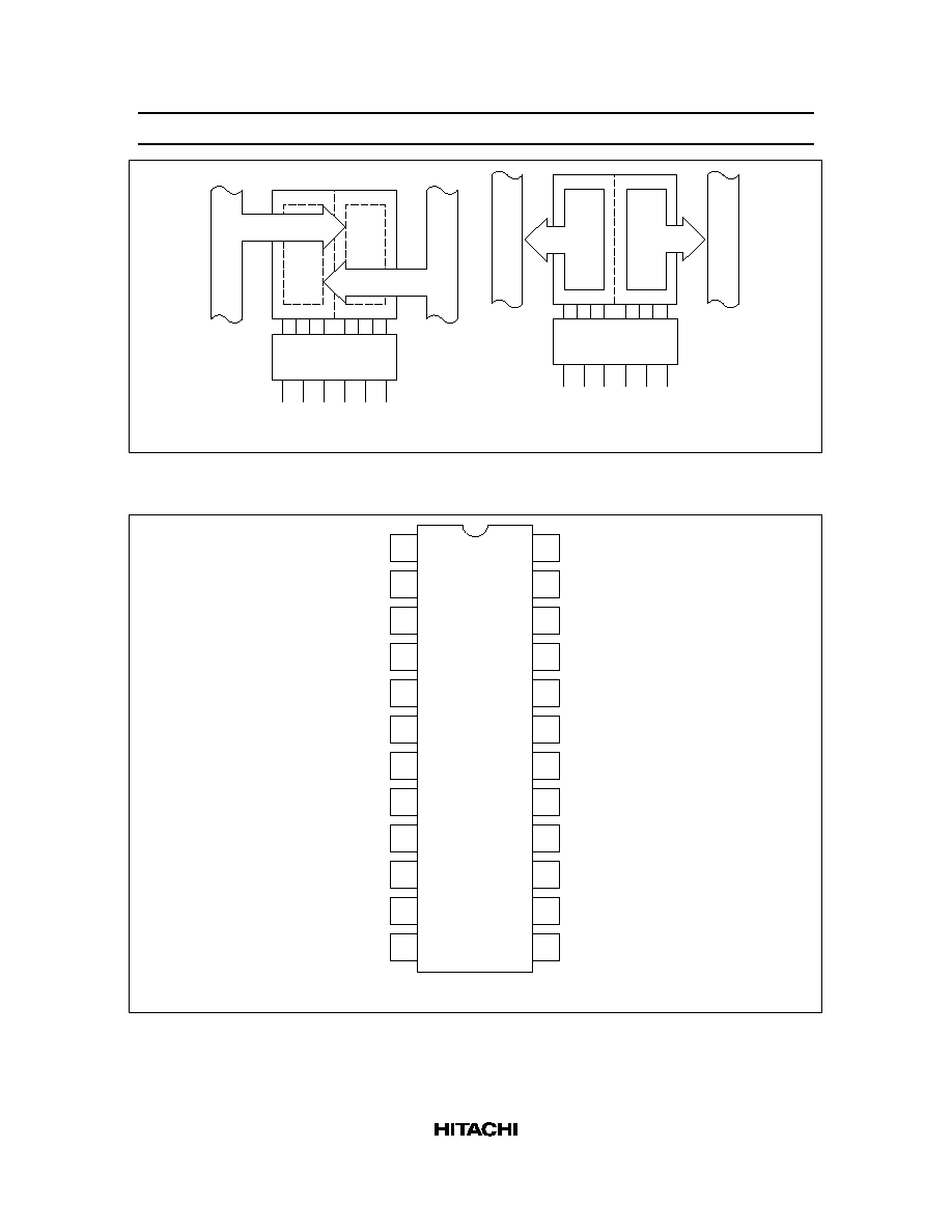
HD74HC651/HD74HC652
Octal Bus Transceivers/Registers (with inverted 3-state outputs)
Octal Bus Transceivers/Registers (with 3-state outputs)
Description
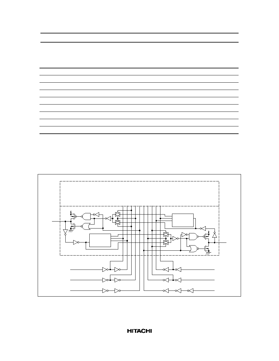
This device consists of bus transceiver circuits, D-type flip-flops, and control circuitry arranged for
multiplexed transmission of data directly from the data bus or from the internal storage registers. Enable
GAB and
GBA are provided to cotrol the transceiver functions. Select AB and Select BA control pins are
provided to select whether real-time or stored data is transferred. A low input level selects real-time data,
and a high selects stored data. The following examples demonstrate the four fundamental bus-management
functions that can be performed with the HD74HC651 and HD74HC652.
Data on the A or B data bus, or both, can be stored in the internal D flip-flops by low-to high transition at
the appropriate clock pins (Clock AB or Clock BA) regardless of the select or enable control pins. When
Select AB and Select BA are in the real-time transfer mode, it is also possible to store data without using
the internal D-type flip-flops by simultaneously enabling Enable GAB and
GBA. In this configuration
each output reinforces its input. Thus, when all other data sources to the two sets of bus lines are at high
impedance, each set of bus lines will remain at its last state.
Features
∑
High Speed Operation: t
pd
(Bus to Bus) = 16 ns typ (C
L
= 50 pF)
∑
High Output Current: Fanout of 15 LSTTL Loads
∑
Wide Operating Voltage: V
CC
= 2 to 6 V
∑
Low Input Current: 1 µA max
∑
Low Quiescent Supply Current: I
CC
(static) = 4 µA max (Ta = 25∞C)

HD74HC651/HD74HC652
2
Function Table
Real-Time Transfer
Bus B to Bus A
Real-Time Transfer
Bus A to Bus B
Storage
Transfer Stored
Data to A and/or B
Clock AB
X
X
L or H
Select AB
X
L
X
H
Enable GAB
L
H
L
H
Clock BA
X
X
L or H
Select BA
L
X
X
H
Enable GBA
L
H
H
L
Bus A
Real-time transfer
Bus B to Bus A
Bus B
Real-time transfer
Bus A to Bus B
Bus A
Bus B