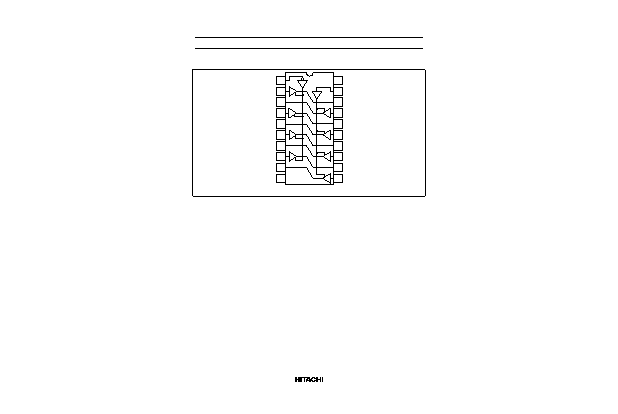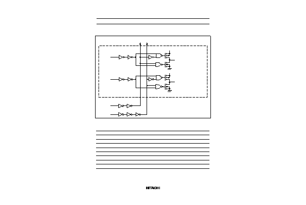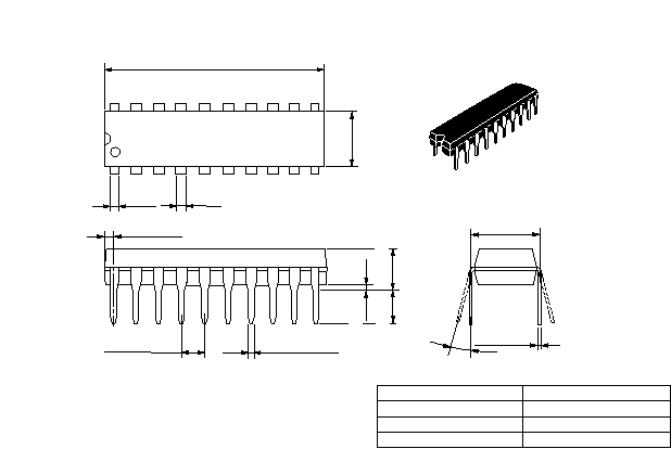
HD74HCT241
Octal Buffers/Line Drivers/Line Receivers
(with noninverted 3-state outputs)
Description
The HD74HCT241 is a noninverting buffer and has one active low enable and one active high enable.
Each enable independently controls 4 buffers.
This device does not have schmitt trigger inputs.
Features
∑
LSTTL Output Logic Level Compatibility as well as CMOS Output Compatibility
∑
High Speed Operation: t
pd
(A to Y) = 10 ns typ (C
L
= 50 pF)
∑
High Output Current: Fanout of 15 LSTTL Loads
∑
Wide Operating Voltage: V
CC
= 4.5 to 5.5 V
∑
Low Input Current: 1 µA max
∑
Low Quiescent Supply Current: I
CC
(static) = 4 µA max (Ta = 25∞C)
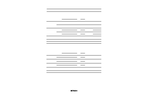
Function Table
Inputs
Output
1
G
2G
A
Y
H
L
X
Z
L
H
H
H
L
H
L
L
H :
High level
L
:
Low level
X :
Irrelevant
Z
:
Off (high impedance) state of a 3-state output