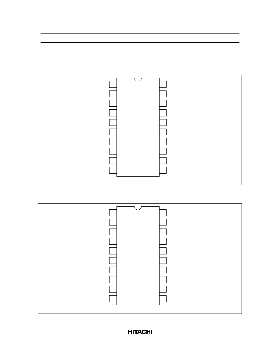
HD74HCT373/HD74HCT533
Octal D-type Transparent Latches (with 3-state outputs)/
Octal D-type Transparent Latches (with inverted 3-state outputs)
Description
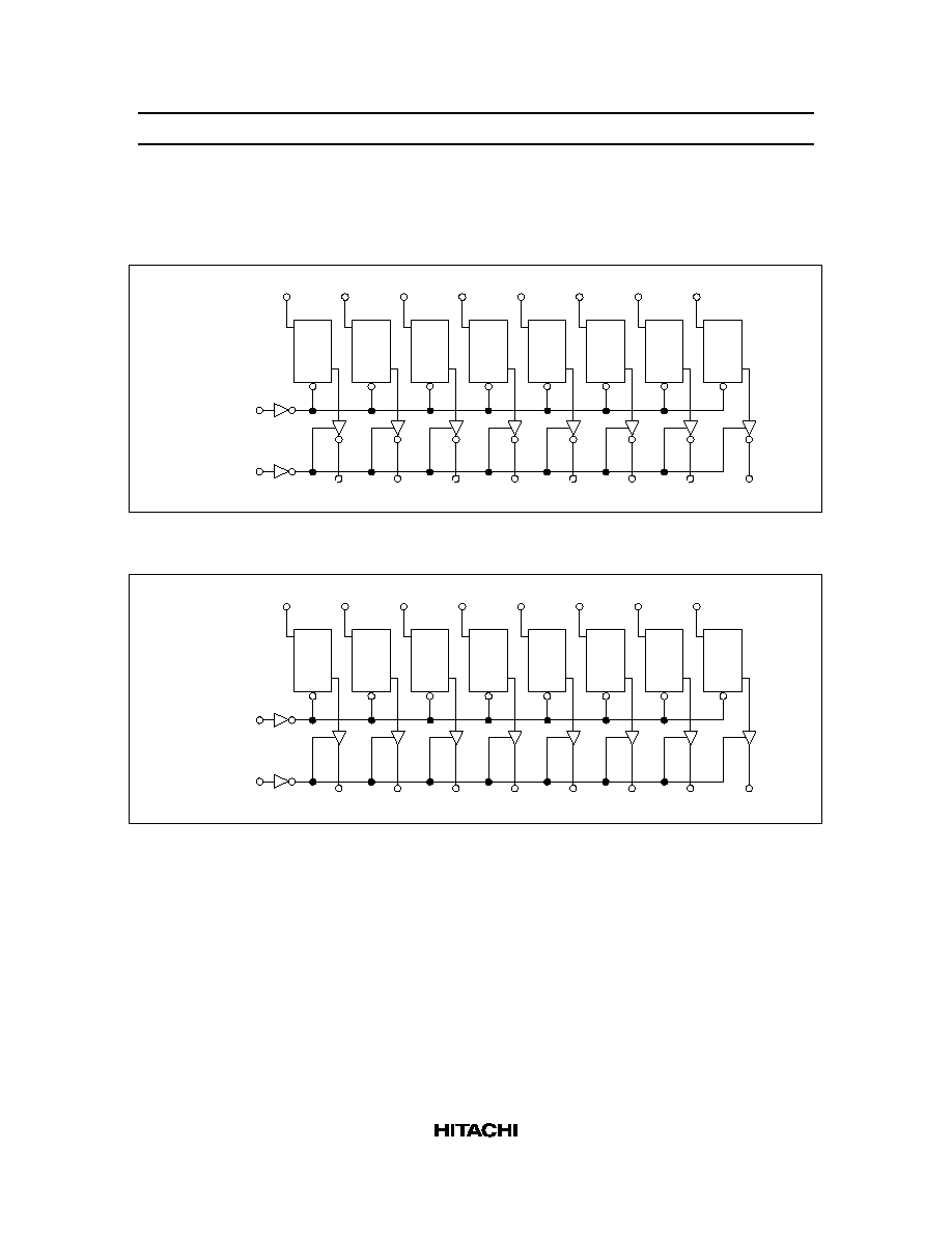
When the latch enable input is high, the Q outputs of HD74HCT373 will follow the D inputs and the Q
outputs of HD74HCT533 will follow the inversion of the D inputs. When the latch enable goes low, data at
the D inputs will be retained at the outputs until latch enable returns high again. When a high logic level is
applied to the output control input, all outputs go to a high impedance state, regardless of what signals
present at the other inputs and the state of the storage elements.
Features
·
LSTTL Output Logic Level Compatibility as well as CMOS Output Compatibility
·
High Speed Operation: t
pd
(Data to Q) = 14 ns typ (C
L
= 50 pF)
·
High Output Current: Fanout of 15 LSTTL Loads
·
Wide Operating Voltage: V
CC
= 4.5 to 5.5 V
·
Low Input Current: 1 µA max
·
Low Quiescent Supply Current: I
CC
(static) = 4 µA max (Ta = 25°C)
Function Table
Output Control
Enable
G
D
HD74HCT373
Q
HD74HCT533
Q
L
H
H
H
L
L
H
L
L
H
L
L
X
No change
No change
H
X
X
Z
Z
X :
Irrelevant
Z
:
Off (high-impedance) state of a 3-state output.