ChipFind - документация

Электронный компонент: HD74HCT573

Скачать:  PDF   ZIP
HD74HCT563/HD74HCT573
Octal Transparent Latches (with 3-state outputs)
Description
When the latch enable (LE) input is high, the Q outputs of HD74HCT563 will follow the inversion of the D
inputs and the Q outputs of HD74HCT573 will follow the D inputs.
When the latch enable goes low, data at the D inputs will be retained at the outputs until latch enabled
returns high again. When a high logic level is applied to the output control input, all outputs go to a high
impedance state, regardless of what signals are present at the other inputs and the state of the storage
elements.
Features
LSTTL Output Logic Level Compatibility as well as CMOS Output Compatibility
High Speed Operation: t
pd
(D to Q,
Q) = 13 ns typ (C
L
= 50 pF)
High Output Current: Fanout of 15 LSTTL Loads
Wide Operating Voltage: V
CC
= 4.5 to 5.5 V
Low Input Current: 1 A max
Low Quiescent Supply Current: I
CC
(static) = 4 A max (Ta = 25C)
Function Table
Outputs
Output Control
Latch Enable
Data
HD74HCT563
HD74HCT573
L
H
H
L
H
L
H
L
H
L
L
L
X
Q
0
Q
0
H
X
X
Z
Z
HD74HCT563/HD74HCT573
2
Pin Arrangement
HD74HCT563
1
2
3
4
5
6
7
8
9
10
1D
2D
3D
4D
5D
6D
7D
8D
GND
20
19
18
17
16
15
14
13
12
11
V
CC
1Q
2Q
3Q
4Q
5Q
6Q
7Q
8Q
Output
Control
OE
Q
D
OE
Q
D
OE
Q
D
OE
Q
D
OE
Q
D
OE
Q
D
OE
Q
D
OE
Q
D
Latch
Enable
(Top view)
HD74HCT563/HD74HCT573
3
HD74HCT573
1
2
3
4
5
6
7
8
9
10
1D
2D
3D
4D
5D
6D
7D
8D
GND
20
19
18
17
16
15
14
13
12
11
V
CC
1Q
2Q
3Q
4Q
5Q
6Q
7Q
8Q
Output
Control
OE
Q
D
OE
Q
D
OE
Q
D
OE
Q
D
OE
Q
D
OE
Q
D
OE
Q
D
OE
Q
D
Latch
Enable
(Top view)
HD74HCT563/HD74HCT573
4
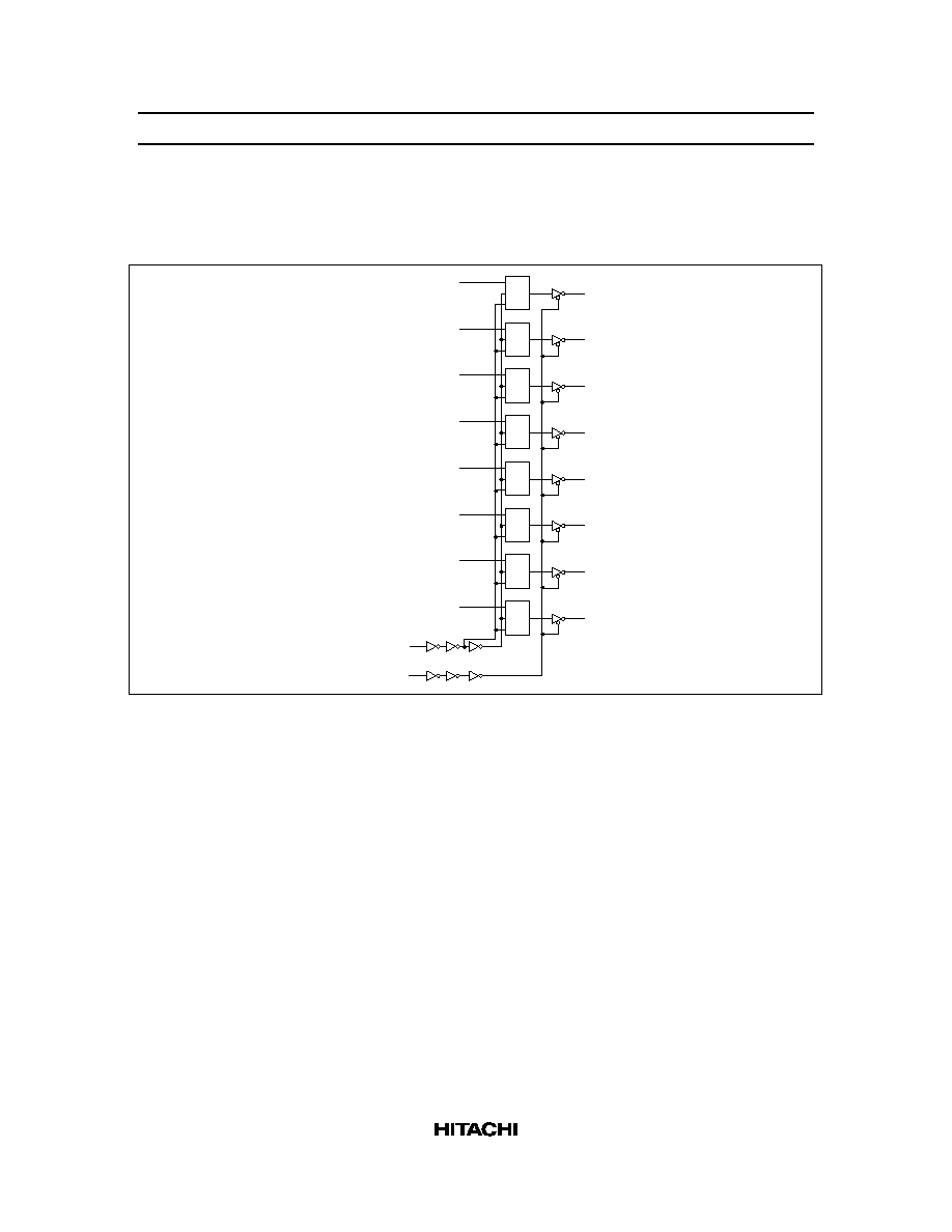
Block Diagram
HD74HCT563
1D
D
C
Q
C
D
C
Q
C
D
C
Q
C
D
C
Q
C
D
C
Q
C
D
C
Q
C
D
C
Q
C
D
C
Q
C
1Q
2Q
3Q
4Q
5Q
6Q
7Q
8Q
2D
3D
4D
6D
7D
8D
5D
Enable C
OC
HD74HCT563/HD74HCT573
5
HD74HCT573
1D
D
C Q
C
D
C Q
C
D
C Q
C
D
C Q
C
D
C Q
C
D
C Q
C
D
C Q
C
D
C Q
C
1Q
2Q
3Q
4Q
5Q
6Q
7Q
8Q
2D
3D
4D
6D
7D
8D
5D
Enable C
OC
Absolute Maximum Ratings
Item
Symbol
Rating
Unit
Supply voltage range
V
CC
0.5 to +7.0
V
Input voltage
V
IN
0.5 to V
CC
+ 0.5
V
Output voltage
V
OUT
0.5 to V
CC
+ 0.5
V
DC current drain per pin
I
OUT
35
mA
DC current drain per V
CC
, GND
I
CC
, I
GND
75
mA
DC input diode current
I
IK
20
mA
DC output diode current
I
OK
20
mA
Power dissipation per package
P
T
500
mW
Storage temperature
Tstg
65 to +150
C