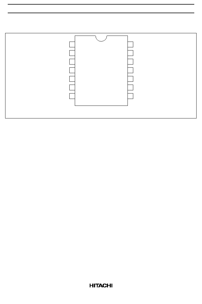
HD74LV132A
Quad. 2-input NAND Schmitt-triggers
ADE-205-260 (Z)
1st Edition
March 1999
Description
The HD74LV132A has four two-input schmitt tigger NAND gates in a 14-pin package.
Low-voltage and high-speed operation is suitable for the battery-powered products (e.g., notebook
computers), and the low-power consumption extends the battery life.
Features
∑
V
CC
= 2.0 V to 5.5 V operation
∑
All inputs V
IH
(Max.) = 5.5 V (@V
CC
= 0 V to 5.5 V)
∑
All outputs V
O
(Max.) = 5.5 V (@V
CC
= 0 V)
∑
Typical V
OL
ground bounce < 0.8 V (@V
CC
= 3.3 V, Ta = 25
∞
C)
∑
Typical V
OH
undershoot > 2.3 V (@V
CC
= 3.3 V, Ta = 25
∞
C)
∑
Output current
±
6 mA (@V
CC
= 3.0 V to 3.6 V),
±
12 mA (@V
CC
= 4.5 V to 5.5 V)
Function Table
Inputs
A
B
Output Y
H
H
L
L
X
H
X
L
H
Note:
H: High level
L: Low level
X: Immaterial

HD74LV132A
3
Absolute Maximum Ratings
Item
Symbol
Ratings
Unit
Conditions
Supply voltage range
V
CC
≠0.5 to 7.0
V
Input voltage range*
1
V
I
≠0.5 to 7.0
V
Output voltage range*
1, 2
V
O
≠0.5 to V
CC
+ 0.5
V
Output: H or L
≠0.5 to 7.0
V
CC
: OFF
Input clamp current
I
IK
≠20
mA
V
I
< 0
Output clamp current
I
OK
±
50
mA
V
O
< 0 or V
O
> V
CC
Continuous output current
I
O
±
25
mA
V
O
= 0 to V
CC
Continuous current through
V
CC
or GND
I
CC
or I
GND
±
50
mA
Maximum power dissipation
at Ta = 25
∞
C (in still air)*
3
P
T
785
mW
SOP
500
TSSOP
Storage temperature
Tstg
≠65 to 150
∞
C
Notes: The absolute maximum ratings are values which must not individually be exceeded, and furthermore,
no two of which may be realized at the same time.
1. The input and output voltage ratings may be exceeded if the input and output clamp-current
ratings are observed.
2. This value is limited to 5.5 V maximum.
3. The maximum package power dissipation was calculated using a junction temperature of 150
∞
C.
HD74LV132A
4
Recommended Operating Conditions
Item
Symbol
Min
Max
Unit
Conditions
Supply voltage range
V
CC
2.0
5.5
V
Input voltage range
V
I
0
5.5
V
Output voltage range
V
O
0
V
CC
V
Output current
I
OH
--
≠50
µ
A
V
CC
= 2.0 V
--
≠2
mA
V
CC
= 2.3 to 2.7 V
--
≠6
V
CC
= 3.0 to 3.6 V
--
≠12
V
CC
= 4.5 to 5.5 V
I
OL
--
50
µ
A
V
CC
= 2.0 V
--
2
mA
V
CC
= 2.3 to 2.7 V
--
6
V
CC
= 3.0 to 3.6 V
--
12
V
CC
= 4.5 to 5.5 V
Operating free-air temperature
Ta
≠40
85
∞
C
Note:
Unused or floating inputs must be held high or low.
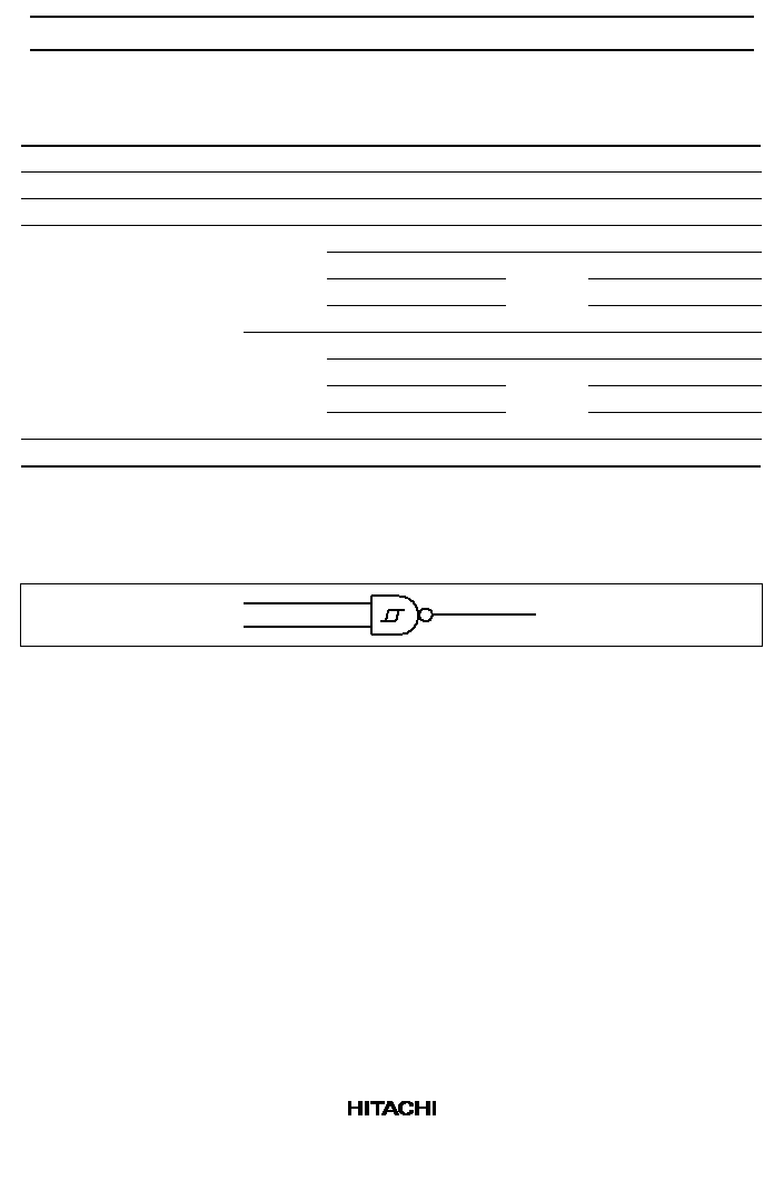
Logic Diagram
A
Y
B