HD74LV161A
Synchronous 4-bit Binary Counter (Direct Clear)
ADE-205-264A (Z)
2nd Edition
June 1999
Description
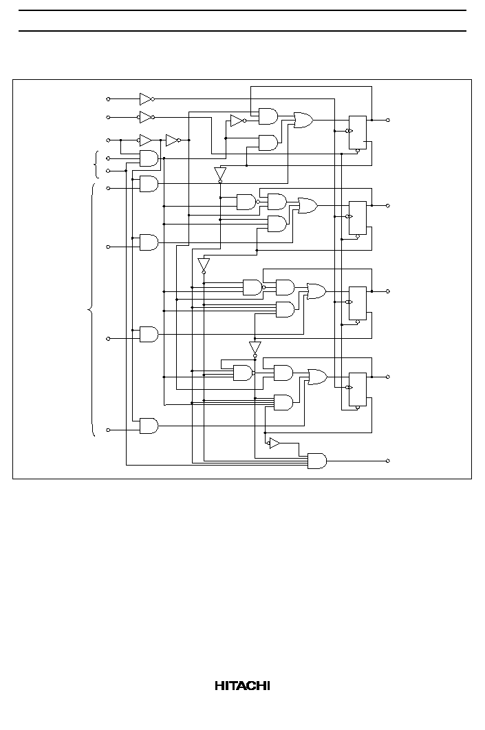
The HD74LV161A is 4-bit binary counters. All flip flops are clocked simultaneously on the low to high to
transition (positive edge) of the clock input waveform. These counters may be preset using the load input.
Presetting of all four flip flops is synchronous to the rising edge of clock. When load is held low counting
is disabled and tha data on the A, B, C and D inputs is loaded into the counter on the rising edge clock. If
the load input is taken high before the positive edge of clock the count operation will be unaffected.
Low-voltage and high-speed operation is suitable for the battery-powered products (e.g., notebook
computers), and the low-power consumption extends the battery life.
Features
∑
V
CC
= 2.0 V to 5.5 V operation
∑
All inputs V
IH
(Max.) = 5.5 V (@V
CC
= 0 V to 5.5 V)
∑
All outputs V
O
(Max.) = 5.5 V (@V
CC
= 0 V)
∑
Typical V
OL
ground bounce < 0.8 V (@V
CC
= 3.3 V, Ta = 25
∞
C)
∑
Typical V
OH
undershoot > 2.3 V (@V
CC
= 3.3 V, Ta = 25
∞
C)
∑
Output current
±
6 mA (@V
CC
= 3.0 V to 3.6 V),
±
12 mA (@V
CC
= 4.5 V to 5.5 V)

HD74LV161A
3
Absolute Maximum Ratings
Item
Symbol
Ratings
Unit
Conditions
Supply voltage range
V
CC
≠0.5 to 7.0
V
Input voltage range*
1
V
I
≠0.5 to 7.0
V
H or L
Output voltage range*
1, 2
V
O
≠0.5 to V
CC
+ 0.5
V
Output: H or L
≠0.5 to 7.0
V
CC
: OFF
Input clamp current
I
IK
≠20
mA
V
I
< 0
Output clamp current
I
OK
±
50
mA
V
O
< 0 or V
O
> V
CC
Continuous output current
I
O
±
25
mA
V
O
= 0 to V
CC
Continuous current through
V
CC
or GND
I
CC
or I
GND
±
50
mA
Maximum power dissipation
at Ta = 25
∞
C (in still air)*
3
P
T
785
mW
SOP
500
TSSOP
Storage temperature
Tstg
≠65 to 150
∞
C
Notes: The absolute maximum ratings are values which must not individually be exceeded, and furthermore,
no two of which may be realized at the same time.
1. The input and output voltage ratings may be exceeded if the input and output clamp-current
ratings are observed.
2. This value is limited to 5.5 V maximum.
3. The maximum package power dissipation was calculated using a junction temperature of 150
∞
C.

HD74LV161A
4
Recommended Operating Conditions
Item
Symbol
Min
Max
Unit
Conditions
Supply voltage range
V
CC
2.0
5.5
V
Input voltage range
V
I
0
5.5
V
Output voltage range
V
O
0
V
CC
V
Output current
I
OH
--
≠50
µ
A
V
CC
= 2.0 V
--
≠2
mA
V
CC
= 2.3 to 2.7 V
--
≠6
V
CC
= 3.0 to 3.6 V
--
≠12
V
CC
= 4.5 to 5.5 V
I
OL
--
50
µ
A
V
CC
= 2.0 V
--
2
mA
V
CC
= 2.3 to 2.7 V
--
6
V
CC
= 3.0 to 3.6 V
--
12
V
CC
= 4.5 to 5.5 V
Input transition rise or fall rate
t /
v
0
200
ns/V
V
CC
= 2.3 to 2.7 V
0
100
V
CC
= 3.0 to 3.6 V
0
20
V
CC
= 4.5 to 5.5 V
Operating free-air temperature
Ta
≠40
85
∞
C
Note:
Unused or floating inputs must be held high or low.