HD74LV175A
Quad. D-type Flip-Flops with Clear
ADE-205-270 (Z)
1st Edition
April 1999
Description
Information at the D inputs of the HD74LV175A is transferred to the Q and
Q outputs on the positive going
edge of the clock pulse. Both true and complement outputs from each flip-flop are externally available.
All four flip-flops are controlled by a common clock and common clear. Clearing is accomplished by a
negative pulse at the clear input. All four Q outputs are cleared to a logic low level and all four
Q outputs
to a logic high level. Low-voltage and high-speed operation is suitable for battery-powered products (e.g.,
notebook computers), and the low-power consumption extends the battery life.
Features
∑
V
CC
= 2.0 V to 5.5 V operation
∑
All inputs V
IH
(Max.) = 5.5 V (@V
CC
= 0 V to 5.5 V)
∑
All outputs V
O
(Max.) = 5.5 V (@V
CC
= 0 V)
∑
Typical V
OL
ground bounce < 0.8 V (@V
CC
= 3.3 V, Ta = 25
∞
C)
∑
Typical V
OH
undershoot > 2.3 V (@V
CC
= 3.3 V, Ta = 25
∞
C)
∑
Output current
±
6 mA (@V
CC
= 3.0 V to 3.6 V),
±
12 mA (@V
CC
= 4.5 V to 5.5 V)
Function Table
Inputs
Outputs
CLR
CLK
D
Q
Q
L
X
X
L
H
H
H
H
L
H
L
L
H
H
X
no change
no change
Note:
H: High level
L: Low level
X: Immaterial
: Low to high transition
: High to low transition
HD74LV175A
2
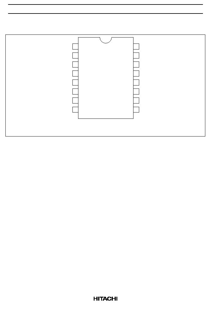
Pin Arrangement
13
14
11
12
15
16
9
10
V
CC
4Q
4
Q
4D
3D
3
Q
1
2
3
4
5
6
7
8
CLR
1Q
1
Q
1D
2D
2
Q
2Q
GND
3Q
CLK
(Top view)
HD74LV175A
3
Absolute Maximum Ratings
Item
Symbol
Ratings
Unit
Conditions
Supply voltage range
V
CC
≠0.5 to 7.0
V
Input voltage range*
1
V
I
≠0.5 to 7.0
V
Output voltage range*
1, 2
V
O
≠0.5 to V
CC
+ 0.5
V
Output: H or L
≠0.5 to 7.0
V
CC
: OFF
Input clamp current
I
IK
≠20
mA
V
I
< 0
Output clamp current
I
OK
±
50
mA
V
O
< 0 or V
O
> V
CC
Continuous output current
I
O
±
25
mA
V
O
= 0 to V
CC
Continuous current through
V
CC
or GND
I
CC
or I
GND
±
50
mA
Maximum power dissipation
at Ta = 25
∞
C (in still air)*
3
P
T
785
mW
SOP
500
TSSOP
Storage temperature
Tstg
≠65 to 150
∞
C
Notes: The absolute maximum ratings are values which must not individually be exceeded, and furthermore,
no two of which may be realized at the same time.
1. The input and output voltage ratings may be exceeded if the input and output clamp-current
ratings are observed.
2. This value is limited to 5.5 V maximum.
3. The maximum package power dissipation was calculated using a junction temperature of 150
∞
C.
HD74LV175A
4
Recommended Operating Conditions
Item
Symbol
Min
Max
Unit
Conditions
Supply voltage range
V
CC
2.0
5.5
V
Input voltage range
V
I
0
5.5
V
Output voltage range
V
O
0
V
CC
V
H or L
Output current
I
OH
--
≠50
µ
A
V
CC
= 2.0 V
--
≠2
mA
V
CC
= 2.3 to 2.7 V
--
≠6
V
CC
= 3.0 to 3.6 V
--
≠12
V
CC
= 4.5 to 5.5 V
I
OL
--
50
µ
A
V
CC
= 2.0 V
--
2
mA
V
CC
= 2.3 to 2.7 V
--
6
V
CC
= 3.0 to 3.6 V
--
12
V
CC
= 4.5 to 5.5 V
Input transition rise or fall rate
t /
v
0
200
ns/V
V
CC
= 2.3 to 2.7 V
0
100
V
CC
= 3.0 to 3.6 V
0
20
V
CC
= 4.5 to 5.5 V
Operating free-air temperature
Ta
≠40
85
∞
C
Note:
Unused or floating inputs must be held high or low.
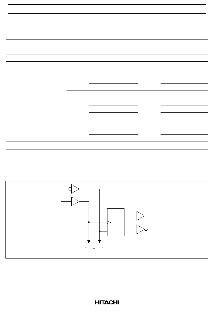
Logic Diagram
CLR
CLK
1D
1D
R
C1
1Q
2
1
Q
3
1
9
3
To Three Other Channels
HD74LV175A
5
DC Electrical Characteristics
∑
Ta = ≠40 to 85
∞
C
Item
Symbol
V
CC
(V)*
Min
Typ
Max
Unit
Test Conditions
Input voltage
V
IH
2.0
1.5
--
--
V
2.3 to 2.7
V
CC
◊
0.7
--
--
3.0 to 3.6
V
CC
◊
0.7
--
--
4.5 to 5.5
V
CC
◊
0.7
--
--
V
IL
2.0
--
--
0.5
2.3 to 2.7
--
--
V
CC
◊
0.3
3.0 to 3.6
--
--
V
CC
◊
0.3
4.5 to 5.5
--
--
V
CC
◊
0.3
Output voltage
V
OH
Min to
Max
V
CC
≠ 0.1
--
--
V
I
OH
= ≠50
µ
A
2.3
2.0
--
--
I
OH
= ≠2 mA
3.0
2.48
--
--
I
OH
= ≠6 mA
4.5
3.8
--
--
I
OH
= ≠12 mA
V
OL
Min to
Max
--
--
0.1
I
OL
= 50
µ
A
2.3
--
--
0.4
I
OL
= 2 mA
3.0
--
--
0.44
I
OL
= 6 mA
4.5
--
--
0.55
I
OL
= 12 mA
Input current
I
IN
0 to 5.5
--
--
±
1
µ
A
V
I
= 5.5 V or GND
Quiescent
supply current
I
CC
5.5
--
--
20
µ
A
V
I
= V
CC
or GND, I
O
= 0
Output leakage
current
I
OFF
0
--
--
5
µ
A
V
I
or V
O
= 0 V to 5.5 V
Input
capacitance
C
IN
3.3
--
1.4
--
pF
V
I
= V
CC
or GND
Note:
For conditions shown as Min or Max, use the appropriate values under recommended operating
conditions.