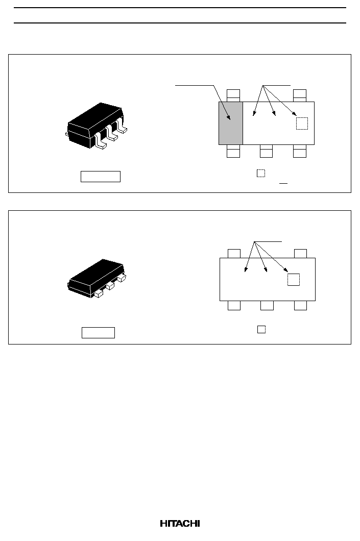
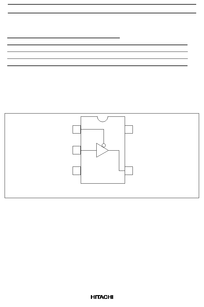
HD74LV1G125A
Bus Buffer Gate with 3≠state Output
ADE-205-323C (Z)
4th. Edition
April 2001
Description
The HD74LV1G125A has a bus buffer gate with 3≠state output in a 5 pin package. Output is disabled
when the associated output enable (
OE) input is high. To ensure the high impedance state during power up
or power down,
OE should be connected to V
CC
through a pull-down resistor; the minimum value of the
resistor is determined by the current souring capability of the driver. Low voltage and high speed operation
is suitable for the battery powered products (e.g., notebook computers), and the low power consumption
extends the battery life.
Features
∑
The basic gate function is lined up as hitachi uni logic series.
∑
Supplied on emboss taping for high speed automatic mounting.
∑
Electrical characteristics equivalent to the HD74LV125A
Supply voltage range : 1.65 to 5.5 V
Operating temperature range : ≠40 to +85
∞
C
∑
All inputs V
IH
(Max.) = 5.5 V (@V
CC
= 0 V to 5.5 V)
All outputs V
O
(Max.) = 5.5 V (@V
CC
= 0 V, Output : Z)
∑
Output current
±
6 mA (@V
CC
= 3.0 V to 3.6 V),
±
12 mA (@V
CC
= 4.5 V to 5.5 V)
∑
All the logical input has hysteresis voltage for the slow transition.
HD74LV1G125A
4
Absolute Maximum Ratings
Item
Symbol
Ratings
Unit
Test Conditions
Supply voltage range
V
CC
≠0.5 to 7.0
V
Input voltage range
*1
V
I
≠0.5 to 7.0
V
Output voltage range
*1, 2
V
O
≠0.5 to V
CC
+ 0.5
V
Output : H or L
≠0.5 to 7.0
V
CC
: OFF or Output : Z
Input clamp current
I
IK
≠20
mA
V
I
< 0
Output clamp current
I
OK
±
50
mA
V
O
< 0 or V
O
> V
CC
Continuous output current
I
O
±
25
mA
V
O
= 0 to V
CC
Continuous current through
V
CC
or GND
I
CC
or I
GND
±
50
mA
Maximum power dissipation
at Ta = 25
∞
C (in still air)
*3
P
T
200
mW
Storage temperature
Tstg
≠65 to 150
∞
C
Notes:
The absolute maximum ratings are values which must not individually be exceeded, and
furthermore no two of which may be realized at the same time.
1. The input and output voltage ratings may be exceeded if the input and output clamp-current
ratings are observed.
2. This value is limited to 5.5 V maximum.
3. The maximum package power dissipation was calculated using a junction temperature of 150
∞
C.
HD74LV1G125A
5
Recommended Operating Conditions
Item
Symbol
Min
Max
Unit
Conditions
Supply voltage range
V
CC
1.65
5.5
V
Input voltage range
V
I
0
5.5
V
Output voltage range
V
O
0
V
CC
V
0
5.5
Output : Z
Output current
I
OL
--
1
mA
V
CC
= 1.65 to 1.95 V
--
2
V
CC
= 2.3 to 2.7 V
--
6
V
CC
= 3.0 to 3.6 V
--
12
V
CC
= 4.5 to 5.5 V
I
OH
--
≠1
V
CC
= 1.65 to 1.95 V
--
≠2
V
CC
= 2.3 to 2.7 V
--
≠6
V
CC
= 3.0 to 3.6 V
--
≠12
V
CC
= 4.5 to 5.5 V
Input transition rise or fall rate
t /
v
0
300
ns / V
V
CC
= 1.65 to 1.95 V
0
200
V
CC
= 2.3 to 2.7 V
0
100
V
CC
= 3.0 to 3.6 V
0
20
V
CC
= 4.5 to 5.5 V
Operating free-air temperature T
a
≠40
85
∞
C
Note:
Unused or floating inputs must be held high or low.