
HD74LV374A
Octal Edge-Triggered D-type Flip-Flops with 3-state Outputs
ADE-205-275 (Z)
1st Edition
April 1999
Description
The HD74LV374A has eight edge trigger D type flip flops with three state outputs in a 20 pin package.
Data at the D inputs meeting set up requirements, are transferred to the Q outputs on positive going
transitions of the clock input. When the clock input goes low, data at the D inputs will be retained at the
outputs until clock input returns high again. When a high logic level is applied to the output control input,
all outputs go to a high impedance state, regardless of what signals are present at the other inputs and the
state of the storage elements. Low-voltage and high-speed operation is suitable for the battery-powered
products (e.g., notebook computers), and the low-power consumption extends the battery life.
Features
∑
V
CC
= 2.0 V to 5.5 V operation
∑
All inputs V
IH
(Max.) = 5.5 V (@V
CC
= 0 V to 5.5 V)
∑
All outputs V
O
(Max.) = 5.5 V (@V
CC
= 0 V)
∑
Typical V
OL
ground bounce < 0.8 V (@V
CC
= 3.3 V, Ta = 25
∞
C)
∑
Typical V
OH
undershoot > 2.3 V (@V
CC
= 3.3 V, Ta = 25
∞
C)
∑
Output current
±
8 mA (@V
CC
= 3.0 V to 3.6 V),
±
16 mA (@V
CC
= 4.5 V to 5.5 V)
Function Table
Inputs
OE
CLK
D
Output Q
H
X
X
Z
L
L
L
L
H
H
L
X
Q
0
Note:
H:
High level
L:
Low level
X:
Immaterial
Z:
High impedance
Q
0
: Output level before the indicated steady state input conditions were established.
HD74LV374A
2
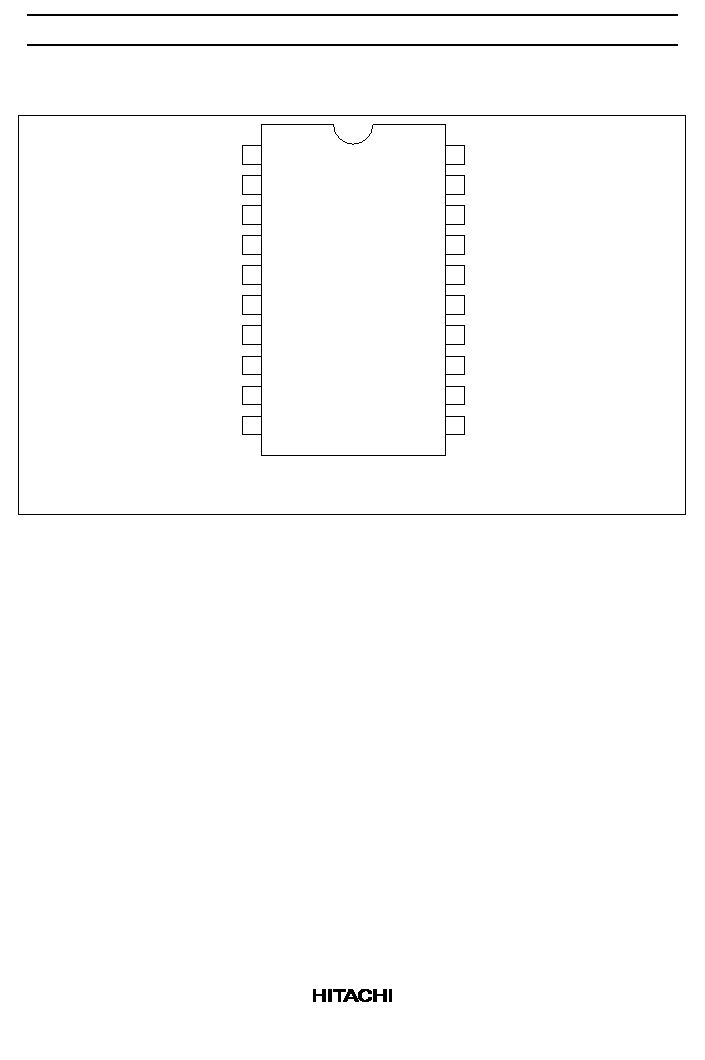
Pin Arrangement
17
18
15
16
19
20
11
12
13
14
V
CC
8Q
8D
7D
7Q
6Q
1
2
3
4
5
6
7
8
9
10
OE
1Q
1D
2D
2Q
3Q
3D
GND
4D
4Q
6D
5D
5Q
CLK
(Top view)
HD74LV374A
3
Absolute Maximum Ratings
Item
Symbol
Ratings
Unit
Conditions
Supply voltage range
V
CC
≠0.5 to 7.0
V
Input voltage range*
1
V
I
≠0.5 to 7.0
V
Output voltage range*
1, 2
V
O
≠0.5 to V
CC
+ 0.5
V
Output: H or L
≠0.5 to 7.0
V
CC
: OFF or Output: Z
Input clamp current
I
IK
≠20
mA
V
I
< 0
Output clamp current
I
OK
±
50
mA
V
O
< 0 or V
O
> V
CC
Continuous output current
I
O
±
35
mA
V
O
= 0 to V
CC
Continuous current through
V
CC
or GND
I
CC
or I
GND
±
70
mA
Maximum power dissipation
at Ta = 25
∞
C (in still air)*
3
P
T
835
mW
SOP
757
TSSOP
Storage temperature
Tstg
≠65 to 150
∞
C
Notes: The absolute maximum ratings are values which must not individually be exceeded, and furthermore,
no two of which may be realized at the same time.
1. The input and output voltage ratings may be exceeded if the input and output clamp-current
ratings are observed.
2. This value is limited to 5.5 V maximum.
3. The maximum package power dissipation was calculated using a junction temperature of 150
∞
C.
HD74LV374A
4
Recommended Operating Conditions
Item
Symbol
Min
Max
Unit
Conditions
Supply voltage range
V
CC
2.0
5.5
V
Input voltage range
V
I
0
5.5
V
Output voltage range
V
O
0
V
CC
V
H or L
0
5.5
High impedance state
Output current
I
OH
--
≠50
µ
A
V
CC
= 2.0 V
--
≠2
mA
V
CC
= 2.3 to 2.7 V
--
≠8
V
CC
= 3.0 to 3.6 V
--
≠16
V
CC
= 4.5 to 5.5 V
I
OL
--
50
µ
A
V
CC
= 2.0 V
--
2
mA
V
CC
= 2.3 to 2.7 V
--
8
V
CC
= 3.0 to 3.6 V
--
16
V
CC
= 4.5 to 5.5 V
Input transition rise or fall rate
t /
v
0
200
ns/V
V
CC
= 2.3 to 2.7 V
0
100
V
CC
= 3.0 to 3.6 V
0
20
V
CC
= 4.5 to 5.5 V
Operating free-air temperature
Ta
≠40
85
∞
C
Note:
Unused or floating inputs must be held high or low.
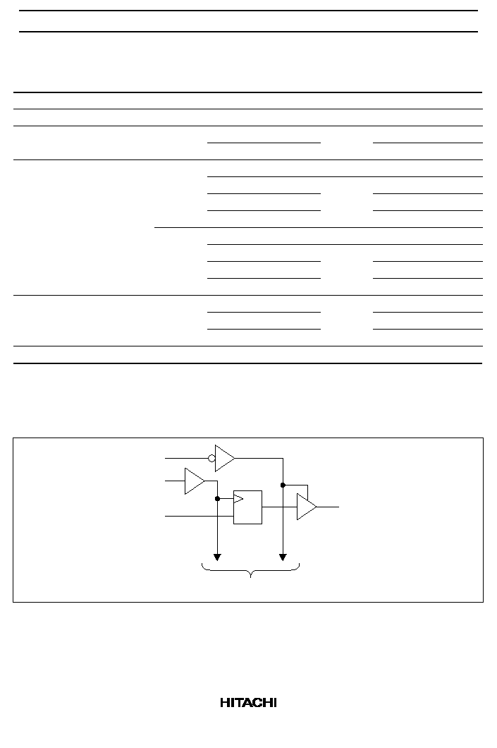
Logic Diagram
To Seven Other Channels
OE
1D
1Q
3
1
2
11
CLK
C1
1D
HD74LV374A
5
DC Electrical Characteristics
∑
Ta = ≠40 to 85
∞
C
Item
Symbol
V
CC
(V)*
Min
Typ
Max
Unit
Test Conditions
Input voltage
V
IH
2.0
1.5
--
--
V
2.3 to 2.7
V
CC
◊
0.7
--
--
3.0 to 3.6
V
CC
◊
0.7
--
--
4.5 to 5.5
V
CC
◊
0.7
--
--
V
IL
2.0
--
--
0.5
2.3 to 2.7
--
--
V
CC
◊
0.3
3.0 to 3.6
--
--
V
CC
◊
0.3
4.5 to 5.5
--
--
V
CC
◊
0.3
Output voltage
V
OH
Min to
Max
V
CC
≠ 0.1
--
--
V
I
OH
= ≠50
µ
A
2.3
2.0
--
--
I
OH
= ≠2 mA
3.0
2.48
--
--
I
OH
= ≠8 mA
4.5
3.8
--
--
I
OH
= ≠16 mA
V
OL
Min to
Max
--
--
0.1
I
OL
= 50
µ
A
2.3
--
--
0.4
I
OL
= 2 mA
3.0
--
--
0.44
I
OL
= 8 mA
4.5
--
--
0.55
I
OL
= 16 mA
Input current
I
IN
0 to 5.5
--
--
±
1
µ
A
V
IN
= 5.5 V or GND
Off-state
output current
I
OZ
5.5
--
--
±
5
µ
A
V
O
= V
CC
or GND
Quiescent
supply current
I
CC
5.5
--
--
20
µ
A
V
IN
= V
CC
or GND, I
O
= 0
Output leakage
current
I
OFF
0
--
--
5
µ
A
V
I
or V
O
= 0 to 5.5 V
Input
capacitance
C
IN
3.3
--
2.9
--
pF
V
I
= V
CC
or GND
Note:
For conditions shown as Min or Max, use the appropriate values under recommended operating
conditions.