HD74LVC16244A
16-bit Buffers / Line Drivers with 3-state Outputs
ADE-205-119B(Z)
3rd Edition
Decemver 1996
Description
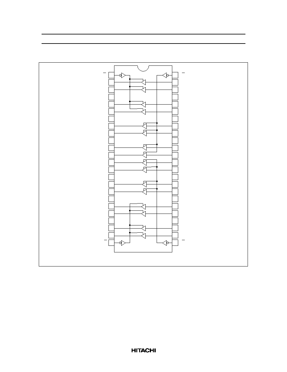
The HD74LVC16244A has sixteen line drivers with three state outputs in a 48 pin package. This device is
a non inverting buffer and has two active low enables (1
G to 4G). Each enable independently controls four
buffers. Low voltage and high speed operation is suitable at the battery drive product (note type personal
computer) and low power consumption extends the life of a battery for long time operation.
Features
∑
V
CC
= 2.0 V to 5.5 V
∑
All inputs V
IH
(Max.) = 5.5 V (@V
CC
= 0 V to 5.5 V)
∑
All outputs V
OUT
(Max.) = 5.5 V (@V
CC
= 0 V or output off state)
∑
Typical V
OL
ground bounce < 0.8 V (@V
CC
= 3.3 V, Ta = 25∞C)
∑
Typical V
OH
undershoot > 2.0 V (@V
CC
= 3.3 V, Ta = 25∞C)
∑
High output current ±24 mA (@V
CC
= 3.0 V to 5.5 V)
Function Table
Inputs
G
A
Output Y
H
X
Z
L
H
H
L
L
L
H:
High level
L:
Low level
X:
Immaterial
Z:
High impedance
HD74LVC16244A
3
Absolute Maximum Ratings
Item
Symbol
Ratings
Unit
Conditions
Supply voltage
V
CC
≠0.5 to 6.0
V
Input diode current
I
IK
≠50
mA
V
I
= ≠0.5 V
Input voltage
V
I
≠0.5 to 6.0
V
Output diode current
I
OK
≠50
mA
V
O
= ≠0.5 V
50
mA
V
O
= V
CC
+0.5 V
Output voltage
V
O
≠0.5 to V
CC
+0.5
V
Output "H" or "L"
≠0.5 to 6.0
V
Output "Z" or V
CC
:OFF
Output current
I
O
±
50
mA
V
CC
, GND current / pin
I
CC
or I
GND
100
mA
Storage temperature
Tstg
≠65 to +150
∞
C
Note:
The absolute maximum ratings are values which must not individually be exceeded, and furthermore,
no two of which may be realized at the same time.
Recommended Operating Conditions
Item
Symbol
Ratings
Unit
Conditions
Supply voltage
V
CC
1.5 to 5.5
V
Data hold
2.0 to 5.5
V
At operation
Input / output voltage
V
I
0 to 5.5
V
G
, A
V
O
0 to V
CC
V
Output "H" or "L"
0 to 5.5
V
Output "Z" or V
CC
:OFF
Operating temperature
Ta
≠40 to 85
∞
C
Output current
I
OH
≠12
mA
V
CC
= 2.7 V
≠24
*2
mA
V
CC
= 3.0 V to 5.5 V
I
OL
12
mA
V
CC
= 2.7 V
24
*2
mA
V
CC
= 3.0 V to 5.5 V
Input rise / fall time
*1
t
r
, t
f
10
ns/V
Notes: 1. This item guarantees maximum limit when one input switches.
Waveform : Refer to test circuit of switching characteristics.
2. duty cycle
50%
HD74LVC16244A
5
Switching Characteristics
Ta = ≠40 to 85
∞
C
Item
Symbol V
CC
(V)
Min
Typ
Max
Unit
From (Input) To (Output)
Propagation delay time
t
PLH
2.7
--
--
5.8
ns
A
Y
t
PHL
3.3
±
0.3
1.5
--
5.2
ns
5.0
±
0.5
--
--
4.0
ns
Output enable time
t
ZH
2.7
--
--
8.2
ns
G
Y
t
ZL
3.3
±
0.3
1.5
--
7.5
ns
5.0
±
0.5
--
--
5.5
ns
Output disable time
t
HZ
2.7
--
--
7.7
ns
G
Y
t
LZ
3.3
±
0.3
1.5
--
7.0
ns
5.0
±
0.5
--
--
6.0
ns
Between output pins skew
*1
t
OSLH
2.7
--
--
--
ns
t
OSHL
3.3
±
0.3
--
--
1.0
ns
5.0
±
0.5
--
--
1.0
ns
Input capacitance
C
IN
2.7
--
3.0
--
pF
Output capacitance
C
O
2.7
--
15.0
--
pF
Note:
1. This parameter is characterized but not tested.
tos
LH
= | t
PLHm
≠ t
PLHn
|, tos
HL
= | t
PHLm
≠ t
PHLn
|
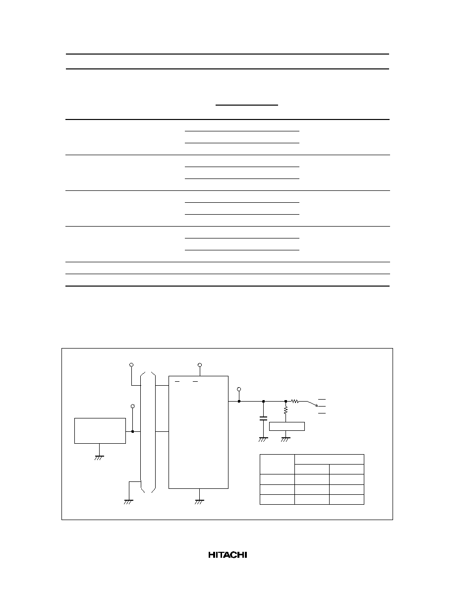
Test Circuit
V
CC
V
CC
See Function Table
1G to 4G
Input
Pulse generator
Z = 50
out
500
C =
50 pF
L
450
OPEN
GND
S1
50 Scope
1A1 to 4A4
1Y1 to 4Y4
Output
*1
See under table
Symbol
S1
t / t
PLH
PHL
OPEN
GND
6 V
t / t
ZH
HZ
t / t
ZL
LZ
OPEN
GND
2
◊
Vcc
Vcc=2.7V,
3.3
±
0.3V
Vcc=5.0
±
0.5V
Note:
1.
C
L
includes probe and jig capacitance.