HD74LVC245A
Octal Bidirectional Transceivers with 3-state Outputs
ADE-205-111B(Z)
3rd Edition
December 1996
Description
The HD74LVC245A has eight buffers with three state outputs in a 20 pin package. When (T /
R) is high,
data flows from the A inputs to the B outputs, and when (T /
R) is low, data flows from the B inputs to the
A outputs. A and B bus are separated by making enable input (
OE) high level. Low voltage and high
speed operation is suitable at the battery drive product (note type personal computer) and low power
consumption extends the life of a battery for long time operation.
Features
∑
V
CC
= 2.0 V to 5.5 V
∑
All inputs V
IH
(Max.) = 5.5 V (@V
CC
= 0 V to 5.5 V)
∑
All input outputs V
I/O
(Max.) = 5.5 V (@V
CC
= 0 V or output off state)
∑
Typical V
OL
ground bounce < 0.8 V (@V
CC
= 3.3 V, Ta = 25∞C)
∑
Typical V
OH
undershoot > 2.0 V (@V
CC
= 3.3 V, Ta = 25∞C)
∑
High output current ±24 mA (@V
CC
= 3.0 V to 5.5 V)
Function Table
Inputs
OE
T /
R
Operation
L
L
B data to A bus
L
H
A data to B bus
H
X
Z
H :
High level
L :
Low level
X :
Immaterial
Z :
High impedance
HD74LVC245A
2
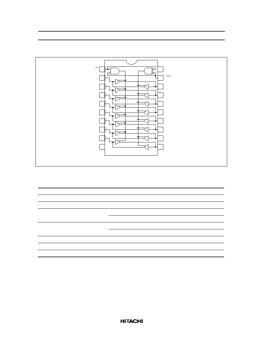
Pin Arrangement
(Top view)
1
2
3
4
5
6
7
8
9
10
11
12
13
14
15
16
17
18
19
20 V
CC
GND
A0
A2
A3
A4
A5
A6
A7
T / R
B1
B2
B3
B4
B5
B6
B7
OE
A1
B0
Absolute Maximum Ratings
Item
Symbol
Ratings
Unit
Conditions
Supply voltage
V
CC
≠0.5 to 6.0
V
Input diode current
I
IK
≠50
mA
V
I
= ≠0.5 V
Input voltage
V
I
≠0.5 to 6.0
V
T /
R
,
OE
Output diode current
I
OK
≠50
mA
V
O
= ≠0.5 V
50
mA
V
O
= V
CC
+0.5 V
Input / output voltage
V
I/O
≠0.5 to V
CC
+0.5
V
Output "H" or "L"
≠0.5 to 6.0
V
Output "Z" or V
CC
:OFF
Output current
I
O
±
50
mA
V
CC
, GND current / pin
I
CC
or I
GND
100
mA
Storage temperature
Tstg
≠65 to 150
∞
C
Note:
The absolute maximum ratings are values which must not individually be exceeded, and furthermore,
no two of which may be realized at the same time.

HD74LVC245A
3
Recommended Operating Conditions
Item
Symbol
Ratings
Unit
Conditions
Supply voltage
V
CC
1.5 to 5.5
V
Data retention
2.0 to 5.5
V
At operation
Input / output voltage
V
I
0 to 5.5
V
T /
R
,
OE
V
I/O
0 to V
CC
V
Output "H" or "L"
0 to 5.5
V
Output "Z" or V
CC
:OFF
Operating temperature
Ta
≠40 to 85
∞
C
Output current
I
OH
≠12
mA
V
CC
= 2.7 V
≠24
*2
mA
V
CC
= 3.0 V to 5.5 V
I
OL
12
mA
V
CC
= 2.7 V
24
*2
mA
V
CC
= 3.0 V to 5.5 V
Input rise / fall time
*1
t
r
, t
f
10
ns/V
Notes: 1. This item guarantees maximum limit when one input switches.
Waveform : Refer to test circuit of switching characteristics.
2. duty cycle
50%