 | ÐлекÑÑоннÑй компоненÑ: HD74LVC32 | СкаÑаÑÑ:  PDF PDF  ZIP ZIP |
Äîêóìåíòàöèÿ è îïèñàíèÿ www.docs.chipfind.ru
HD74LVC32
Quad. 2-input OR Gates
ADE-205-065B(Z)
Rev.2
September 1995
Description
The HD74LVC32 has four 2-input OR gates in a 14 pin package. Low voltage and high speed operation is
suitable at the battery drive product (note type personal computer) and low power consumption extends the
life of a battery for long time operation.
Features
·
V
CC
= 2.0 V to 5.5 V
·
All inputs V
IH
(Max.) = 5.5 V (@V
CC
= 0 V to 5.5 V)
·
Typical V
OL
ground bounce < 0.8 V (@V
CC
= 3.3 V, Ta = 25°C)
·
Typical V
OH
undershoot > 2.0 V (@V
CC
= 3.3 V, Ta = 25°C)
·
High output current ±24 mA (@V
CC
= 3.0 V to 5.5 V)
Function Table
Inputs
A
B
Output Y
L
L
L
H
L
H
L
H
H
H
H
H
H :
High level
L :
Low level
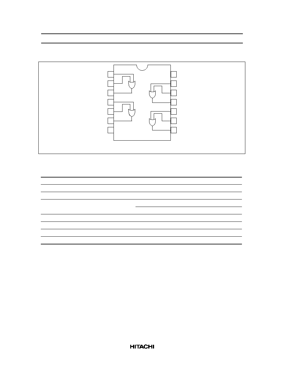
HD74LVC32
2
Pin Arrangement
(Top view)
11
12
13
14 V
CC
4B
4A
4Y
3B
3A
1
2
3
4
5
6
7
8
9
10
1A
GND
3Y
1B
1Y
2A
2B
2Y
Absolute Maximum Ratings
Item
Symbol
Ratings
Unit
Conditions
Supply voltage range
V
CC
0.5 to 6.0
V
Input diode current
I
IK
50
mA
V
I
= 0.5 V
Input voltage
V
I
0.5 to 6.0
V
Output diode current
I
OK
50
mA
V
O
= 0.5 V
50
mA
V
O
= V
CC
+0.5 V
Output voltage
V
O
0.5 to V
CC
+0.5
V
Output current
I
O
±
50
mA
V
CC
, GND current / pin
I
CC
or I
GND
100
mA
Storage temperature
Tstg
65 to +150
°
C
Note:
The absolute maximum ratings are values which must not individually be exceeded, and furthermore,
no two of which may be realized at the same time.
HD74LVC32
3
Recommended Operating Conditions
Item
Symbol
Ratings
Unit
Conditions
Supply voltage
V
CC
1.5 to 5.5
V
Data retention
2.0 to 5.5
V
At operation
Input / Output voltage
V
I
0 to 5.5
V
A, B
V
O
0 to V
CC
V
Y
Operating temperature
Ta
40 to 85
°
C
Output current
I
OH
12
mA
V
CC
= 2.7 V
24
*2
mA
V
CC
= 3.0 V to 5.5 V
I
OL
12
mA
V
CC
= 2.7 V
24
*2
mA
V
CC
= 3.0 V to 5.5 V
Input rise / fall time
*1
t
r
, t
f
10
ns/V
Notes: 1. This item guarantees maximum limit when one input switches.
Waveform : Refer to test circuit of switching characteristics.
2. duty cycle
50%
Electrical Characteristics
Ta = 40 to 85
°
C
Item
Symbol V
CC
(V)
Min
Max
Unit Test Conditions
Input voltage
V
IH
2.7 to 3.6
2.0
--
V
4.5 to 5.5
V
CC
×
0.7
--
V
V
IL
2.7 to 3.6
--
0.8
V
4.5 to 5.5
--
V
CC
×
0.3
V
Output voltage
V
OH
2.7 to 5.5
V
CC
0.2 --
V
I
OH
= 100
µ
A
2.7
2.2
--
V
I
OH
= 12 mA
3.0
2.4
--
V
I
OH
= 12 mA
3.0
2.0
--
V
I
OH
= 24 mA
4.5
3.8
--
V
I
OH
= 24 mA
V
OL
2.7 to 5.5
--
0.2
V
I
OL
= 100
µ
A
2.7
--
0.4
V
I
OL
= 12 mA
3.0
--
0.55
V
I
OL
= 24 mA
4.5
--
0.55
V
I
OL
= 24 mA
Input current
I
IN
0 to 5.5
--
±
5.0
µ
A
V
IN
= 5.5 V or GND
Quiescent supply current I
CC
5.5
--
20
µ
A
V
IN
= V
CC
or GND
I
CC
3.0 to 3.6
--
500
µ
A
V
IN
= one input at (V
CC
0.6)V,
other inputs at V
CC
or GND
HD74LVC32
4
Switching Characteristics
Ta = 40 to 85
°
C
Item
Symbol
V
CC
(V)
Min
Typ
Max
Unit
From (Input) To (Output)
Propagation delay time
t
PLH
2.7
--
4.5
7.0
ns
A or B
Y
t
PHL
3.3
±
0.3
1.5
3.5
6.0
ns
5.0
±
0.5
--
3.0
5.0
ns
Input capacitance
C
IN
2.7
--
3.0
--
pF
Output capacitance
C
O
2.7
--
15.0
--
pF
HD74LVC32
5
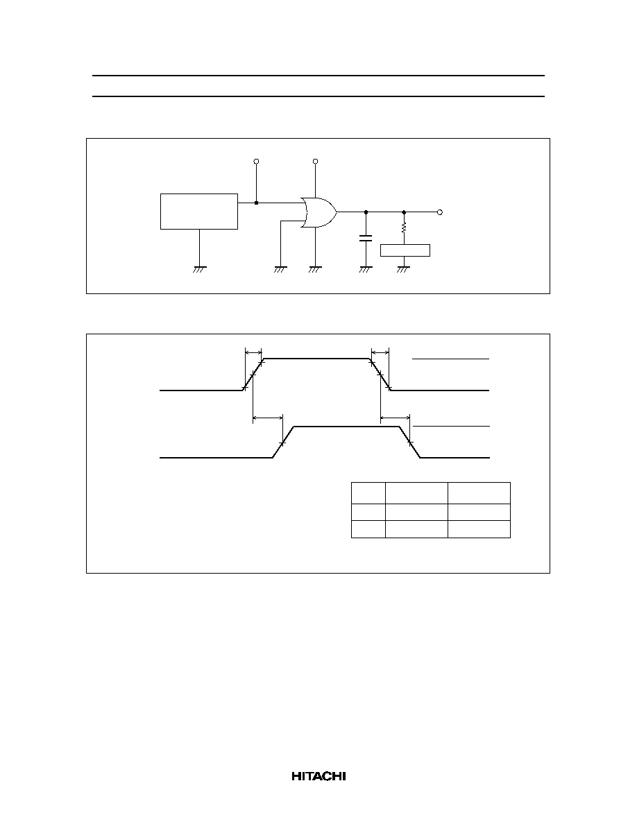
Test Circuit
Input
Pulse Generator
Z = 50
out
V
CC
Output
C =
50 pF
L
50 Scope
450
Note:
1.
C
L
includes probe and jig capacitance.
Waveforms
t
PLH
t
PHL
V
OH
V
OL
Input A or B
10 %
GND
90 %
t
r
t
f
90 %
10 %
Output Y
V
IH
V
ref
V
2.7 V
1.5 V
IH
V
ref
Symbol
V
CC
= 2.7 V,
3.3
±
0.3 V
V
CC
= 5.0
±
0.5 V
V
CC
50%V
CC
V
ref
V
ref
V
ref
Notes: 1.
t
r
= 2.5 ns, t
f
= 2.5 ns
2.
Input waveform : PRR = 10 MHz, duty cycle 50%.