 | –≠–ª–µ–∫—Ç—Ä–æ–Ω–Ω—ã–π –∫–æ–º–ø–æ–Ω–µ–Ω—Ç: HD74LVC74 | –°–∫–∞—á–∞—Ç—å:  PDF PDF  ZIP ZIP |
HD74LVC74
Dual D-type Flip Flops with Preset and Clear
ADE-205-066C(Z)
Rev.3
September 1995
Description
The HD74LVC74 has independent data, preset, clear, and clock inputs Q and
Q outputs in a 14 pin
package. The logic level present at the data input is transferred to the output during the positive going
transition of the clock pulse. Preset and clear are independent of the clock and accomplished by a low level
at the appropriate input. Low voltage and high speed operation is suitable at the battery drive product (note
type personal computer) and low power consumption extends the life of a battery for long time operation.
Features
∑
V
CC
= 2.0 V to 5.5 V
∑
All inputs V
IH
(Max.) = 5.5 V (@V
CC
= 0 V to 5.5 V)
∑
Typical V
OL
ground bounce < 0.8 V (@V
CC
= 3.3 V, Ta = 25∞C)
∑
Typical V
OH
undershoot > 2.0 V (@V
CC
= 3.3 V, Ta = 25∞C)
∑
High output current ±24 mA (@V
CC
= 3.0 V to 5.5 V)
HD74LVC74
2
Function Table
Inputs
Outputs
PR
CLR
CK
D
Q
Q
L
H
X
X
H
L
H
L
X
X
L
H
L
L
X
X
H
*1
H
*1
H
H
H
H
L
H
H
L
L
H
H
H
L
X
Q
0
Q
0
H
H
H
X
Q
0
Q
0
H
H
X
Q
0
Q
0
H :
High level
L :
Low level
X :
Immaterial
:
High to Low transition
:
Low to high transition
Q
0
:
Level to Q before the indicated steady input conditions were established.
Note:
1. Q and
Q
will remain high as long as preset and clear are low, but Q and
Q
are unpredictable, if
preset and clear go high simultaneously.
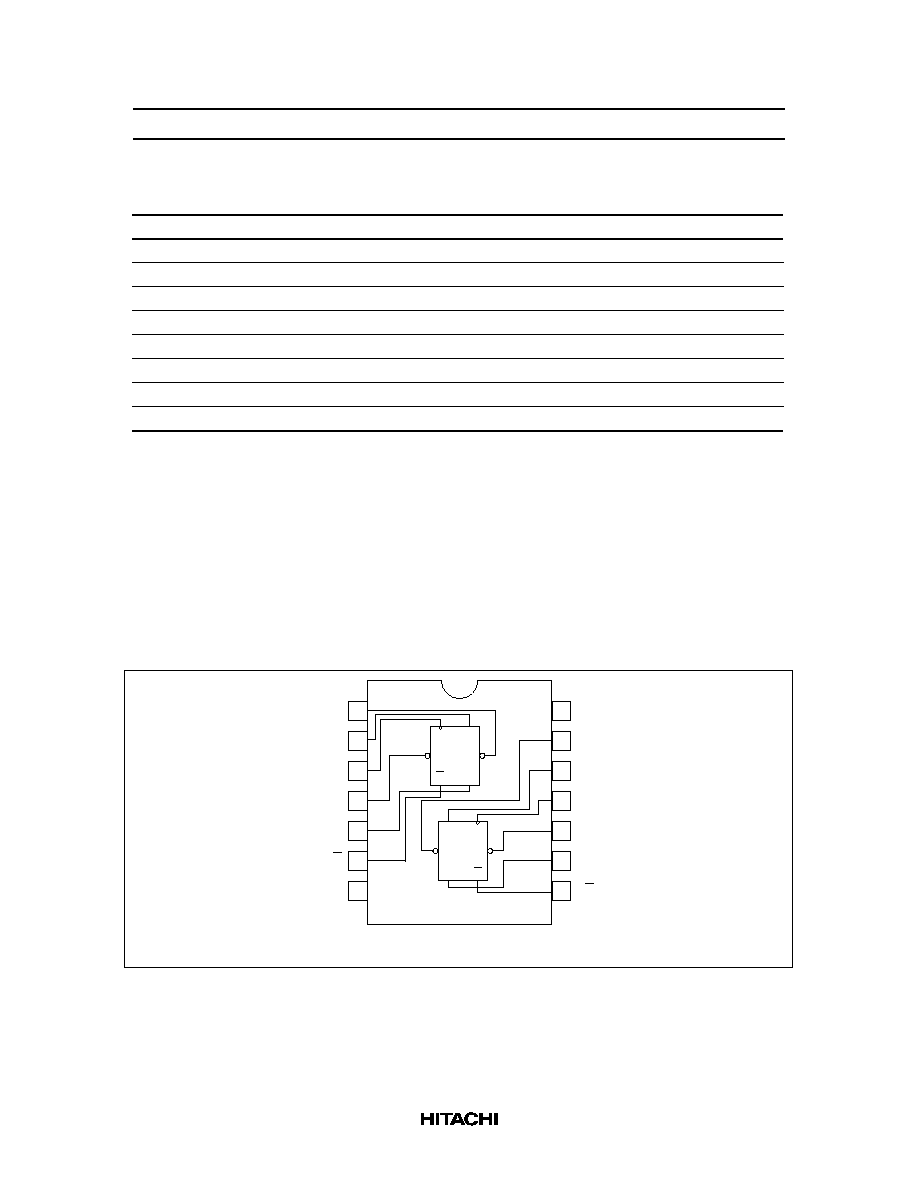
Pin Arrangement
(Top view)
11
12
13
14 V
CC
2CLR
2D
2CK
2PR
2Q
1
2
3
4
5
6
7
8
9
10
1CLR
GND
1D
1CK
1PR
1Q
1Q
2Q
D
CK
PR CLR
Q
Q
D
CK
CLR
PR
Q
Q
HD74LVC74
3
Absolute Maximum Ratings
Item
Symbol
Ratings
Unit
Conditions
Supply voltage
V
CC
≠0.5 to 6.0
V
Input diode current
I
IK
≠50
mA
V
I
= ≠0.5 V
Input voltage
V
I
≠0.5 to 6.0
V
Output diode current
I
OK
≠50
mA
V
O
= ≠0.5 V
50
mA
V
O
= V
CC
+0.5 V
Output voltage
V
O
≠0.5 to V
CC
+0.5 V
Output current
I
O
±
50
mA
V
CC
, GND current / pin
I
CC
or I
GND
100
mA
Storage temperature
Tstg
≠65 to +150
∞
C
Note:
The absolute maximum ratings are values which must not individually be exceeded, and furthermore,
no two of which may be realized at the same time.
Recommended Operating Conditions
Item
Symbol
Ratings
Unit
Conditions
Supply voltage
V
CC
1.5 to 5.5
V
Data retention
2.0 to 5.5
V
At operation
Input / output voltage
V
I
0 to 5.5
V
PR, CLR, CK, D
V
O
0 to V
CC
V
Q,
Q
Operating temperature
Ta
≠40 to 85
∞
C
Output current
I
OH
≠12
mA
V
CC
= 2.7 V
≠24
*2
mA
V
CC
= 3.0 V to 5.5 V
I
OL
12
mA
V
CC
= 2.7 V
24
*2
mA
V
CC
= 3.0 V to 5.5 V
Input rise / fall time
*1
t
r
,
t
f
10
ns/V
Notes: 1. This item guarantees maximum limit when one input switches.
Waveform : Refer to test circuit of switching characteristics.
2. duty cycle
50%

HD74LVC74
4
Electrical Characteristics
Ta = ≠40 to 85
∞
C
Item
Symbol V
CC
(V)
Min
Max
Unit Test Conditions
Input voltage
V
IH
2.7 to 3.6
2.0
--
V
4.5 to 5.5
V
CC
◊
0.7
--
V
V
IL
2.7 to 3.6
--
0.8
V
4.5 to 5.5
--
V
CC
◊
0.3
V
Output voltage
V
OH
2.7 to 5.5
V
CC
≠0.2 --
V
I
OH
= ≠100
µ
A
2.7
2.2
--
V
I
OH
= ≠12 mA
3.0
2.4
--
V
3.0
2.0
--
V
I
OH
= ≠24 mA
4.5
3.8
--
V
V
OL
2.7 to 5.5
--
0.2
V
I
OL
= 100
µ
A
2.7
--
0.4
V
I
OL
= 12 mA
3.0
--
0.55
V
I
OL
= 24 mA
4.5
--
0.55
V
Input current
I
IN
0 to 5.5
--
±
5.0
µ
A
V
IN
= 5.5 V or GND
Quiescent supply current I
CC
5.5
--
20
µ
A
V
IN
= V
CC
or GND
I
CC
3.0 to 3.6
--
500
µ
A
V
IN
= one input at (V
CC
≠0.6)V,
other inputs at V
CC
or GND
HD74LVC74
5
Switching Characteristics
Ta = ≠40 to 85
∞
C
Item
Symbol
V
CC
(V)
Min
Typ
Max
Unit From (Input)
To (Output)
Maximum clock frequency f
max
2.7
150.0 --
--
MHz
3.3
±
0.3
150.0 --
--
MHz
5.0
±
0.5
150.0 --
--
MHz
Propagation delay time
t
PLH
2.7
--
6.0
9.0
ns
CLK
Q,
Q
t
PHL
3.3
±
0.3
1.5
5.0
8.0
ns
5.0
±
0.5
--
4.0
6.5
ns
t
PLH
2.7
--
6.5
9.0
ns
PR or CLR
Q,
Q
t
PHL
3.3
±
0.3
1.5
5.0
8.0
ns
5.0
±
0.5
--
4.0
6.5
ns
Setup time
t
su
2.7
4.0
--
--
ns
3.3
±
0.3
3.0
--
--
ns
5.0
±
0.5
3.0
--
--
ns
Hold time
t
h
2.7
2.0
--
--
ns
3.3
±
0.3
2.0
--
--
ns
5.0
±
0.5
2.0
--
--
ns
Pulse width
t
w
2.7
4.0
--
--
ns
CK
3.3
±
0.3
4.0
--
--
ns
5.0
±
0.5
4.0
--
--
ns
2.7
6.0
--
--
ns
PR or CLR
3.3
±
0.3
5.0
--
--
ns
5.0
±
0.5
4.0
--
--
ns
Recovery time
t
rec
2.7
3.0
--
--
ns
3.3
±
0.3
2.0
--
--
ns
5.0
±
0.5
2.0
--
--
ns
Input capacitance
C
IN
2.7
--
3.0
--
pF
Output capacitance
C
O
2.7
--
15.0
--
pF