HM5112805F-6, HM5113805F-6
128M EDO DRAM (16-Mword
◊
8-bit)
8k refresh/4k refresh
ADE-203-1050C (Z)
Rev. 3.0
Feb. 2, 2000
Description
The Hitachi HM5112805F, HM5113805F are 128M-bit dynamic RAMs organized as 16,777,216-word
◊
8-bit. They have realized high performance and low power by employing CMOS process technology.
HM5112805F, HM5113805F offer Extended Data Out (EDO) Page Mode as a high speed access mode.
They are packaged in 32-pin plastic TSOPII.
Features
∑
Single 3.3 V supply: 3.3 V
±
0.3 V
∑
Access time: 60 ns (max)
∑
Power dissipation
Active:
720 mW (max) (HM5112805F)
792 mW (max) (HM5113805F)
Standby : 3.6 mW (max) (CMOS interface)
: 1.8 mW (max) (CMOS interface) (L-version)
∑
EDO page mode capability
∑
Refresh cycles
RAS-only refresh
8192 cycles/64 ms (HM5112805F)
4096 cycles/64 ms (HM5113805F)
CBR/Hidden refresh
4096 cycles/64 ms (HM5112805F, HM5113805F)
HM5112805F-6, HM5113805F-6
2
∑
4 variations of refresh
RAS-only refresh
CAS-before-RAS refresh
Hidden refresh
Self refresh (L-version)
∑
Battery backup operation (L-version)
Ordering Information
Type No.
Access time
Package
HM5112805FTD-6
60 ns
400-mil 32-pin plastic TSOP II (TTP-32DF)
HM5112805FLTD-6
60 ns
HM5113805FTD-6
60 ns
HM5113805FLTD-6
60 ns
HM5112805F-6, HM5113805F-6
3
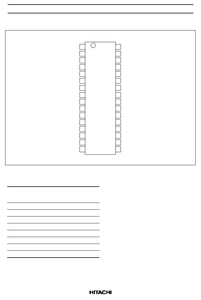
Pin Arrangement (HM5112805F)
(Top view)
32-pin TSOP
1
2
3
4
5
6
7
8
9
10
11
12
13
14
15
16
32
31
30
29
28
27
26
25
24
23
22
21
20
19
18
17
V
CC
I/O0
I/O1
I/O2
I/O3
NC
V
CC
WE
RAS
A0
A1
A2
A3
A4
A5
V
CC
V
SS
I/O7
I/O6
I/O5
I/O4
V
SS
CAS
OE
A12
A11
A10
A9
A8
A7
A6
V
SS
Pin Description
Pin name
Function
A0 to A12
Address input
-- Row/Refresh address A0 to A12
-- Column address
A0 to A10
I/O0 to I/O7
Data input/output
RAS
Row address strobe
CAS
Column address strobe
WE
Write enable
OE
Output enable
V
CC
Power supply
V
SS
Ground
NC
No connection
HM5112805F-6, HM5113805F-6
4
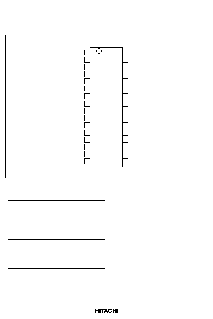
Pin Arrangement (HM5113805F)
(Top view)
32-pin TSOP
1
2
3
4
5
6
7
8
9
10
11
12
13
14
15
16
32
31
30
29
28
27
26
25
24
23
22
21
20
19
18
17
V
CC
I/O0
I/O1
I/O2
I/O3
NC
V
CC
WE
RAS
A0
A1
A2
A3
A4
A5
V
CC
V
SS
I/O7
I/O6
I/O5
I/O4
V
SS
CAS
OE
NC
A11
A10
A9
A8
A7
A6
V
SS
Pin Description
Pin name
Function
A0 to A11
Address input
-- Row/Refresh address A0 to A11
-- Column address
A0 to A11
I/O0 to I/O7
Data input/output
RAS
Row address strobe
CAS
Column address strobe
WE
Write enable
OE
Output enable
V
CC
Power supply
V
SS
Ground
NC
No connection
HM5112805F-6, HM5113805F-6
5
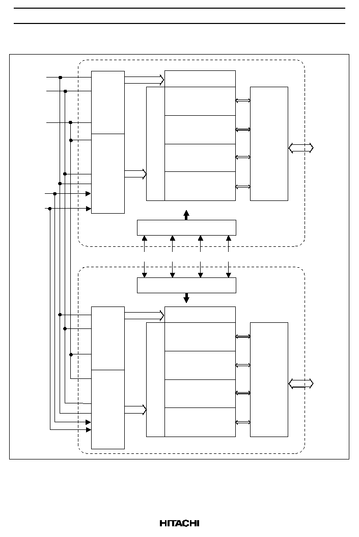
Block Diagram (HM5112805F)
Timing and control
Timing and control
Column
address
buffers
Row
address
buffers
I/O buffers
∑
∑
∑
∑
∑
∑
A0
A1
to
A10
A11
A12
I/O1
I/O3
I/O4
I/O6
RAS
CAS
WE
OE
Column decoder
Row decoder
16M array
16M array
16M array
16M array
Column
address
buffers
Row
address
buffers
I/O buffers
I/O0
I/O2
I/O5
I/O7
Column decoder
Row decoder
16M array
16M array
16M array
16M array
Upper pellet
Lower pellet