
HM514260C Series
HM51S4260C Series
262,144-word
◊
16-bit Dynamic Random Access Memory
ADE-203-260A (Z)
Rev. 1.0
Jun. 12, 1995
Description
The Hitachi HM51(S)4260C is CMOS dynamic RAM organized as 262,144-word
◊
16-bit. HM51(S)4260C
has realized higher density, higher performance and various functions by employing 0.8
µ
m CMOS process
technology and some new CMOS circuit design technologies. The HM51(S)4260C offers fast page mode as a
high speed access mode. Multiplexed address input permits the HM51(S)4260C to be packaged in standard
400-mil 40-pin plastic SOJ and standard 400-mil 44-pin plastic TSOPII. Internal refresh timer enables
HM51S4260C self refresh operation.
Features
∑
Single 5 V (
±
10%) (HM51(S)4260C-6/7/8)
(
±
5%) (HM51(S)4260C-6R)
∑
High speed
-- Access time: 60 ns/70 ns/80 ns (max)
∑
Low power dissipation
-- Active mode: 825 mW/788 mW/770 mW/688 mW (max)
-- Standby mode: 11 mW (max) (HM51(S)4260C-6/7/8)
10.5 mW (max) (HM51(S)4260C-6R)
1.1 mW (max) (L-version) (HM51(S)4260C-6/7/8)
1.05 mW (max) (L-version) (HM51(S)4260C-6R)
∑
Fast page mode capability
∑
512 refresh cycles: 8 ms
128 ms (L-version)
∑
2 CAS-byte control
∑
2 variations of refresh
-- RAS-only refresh
-- CAS-before-RAS refresh
∑
Battery backup operation (L-version)
∑
Self refresh operation (HM51S4260C)

HM514260C, HM51S4260C Series
2
Ordering Information
Type No.
Access Time
Package
HM514260CJ-6
HM514260CJ-6R
HM514260CJ-7
HM514260CJ-8
60 ns
60 ns
70 ns
80 ns
400-mill 40-pin plastic SOJ (CP-40DA)
HM514260CLJ-6
HM514260CLJ-6R
HM514260CLJ-7
HM514260CLJ-8
60 ns
60 ns
70 ns
80 ns
HM51S4260CJ-6
HM51S4260CJ-6R
HM51S4260CJ-7
HM51S4260CJ-8
60 ns
60 ns
70 ns
80 ns
HM51S4260CLJ-6
HM51S4260CLJ-6R
HM51S4260CLJ-7
HM51S4260CLJ-8
60 ns
60 ns
70 ns
80 ns
HM514260CTT-6
HM514260CTT-6R
HM514260CTT-7
HM514260CTT-8
60 ns
60 ns
70 ns
80 ns
400-mill 44-pin plastic TSOP II (TTP-44/40DB)
HM514260CLTT-6
HM514260CLTT-6R
HM514260CLTT-7
HM514260CLTT-8
60 ns
60 ns
70 ns
80 ns
HM51S4260CTT-6
HM51S4260CTT-6R
HM51S4260CTT-7
HM51S4260CTT-8
60 ns
60 ns
70 ns
80 ns
HM51S4260CLTT-6
HM51S4260CLTT-6R
HM51S4260CLTT-7
HM51S4260CLTT-8
60 ns
60 ns
70 ns
80 ns
HM514260C, HM51S4260C Series
3
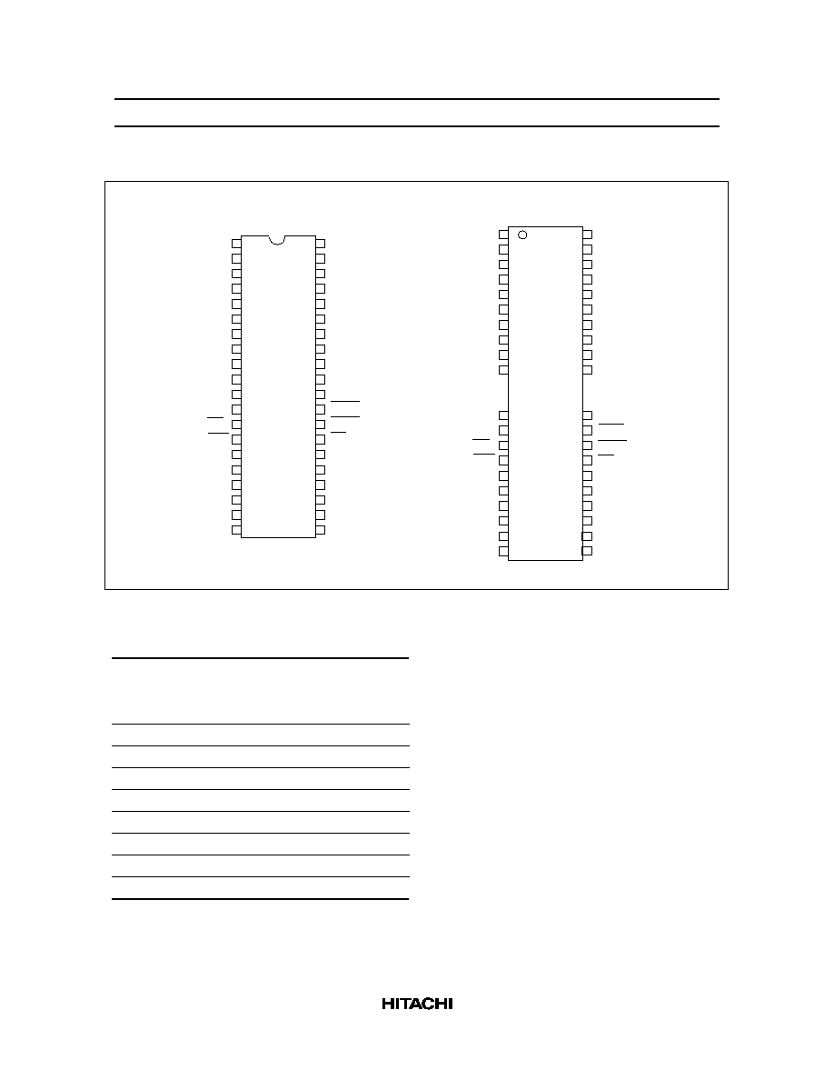
Pin Arrangement
V
I/O0
I/O1
I/O2
I/O3
V
I/O4
I/O5
I/O6
I/O7
NC
NC
WE
RAS
NC
A0
A1
A2
A3
V
CC
CC
CC
V
I/O15
I/O14
I/O13
I/O12
V
I/O11
I/O10
I/O9
I/O8
NC
LCAS
UCAS
OE
A8
A7
A6
A5
A4
V
SS
SS
SS
1
2
3
4
5
6
7
8
9
10
11
12
13
14
15
16
17
18
19
20
40
39
38
37
36
35
34
33
32
31
30
29
28
27
26
25
24
23
22
21
(Top view)
HM514260CJ/CLJ Series
HM51S4260CJ/CLJ Series
V
I/O0
I/O1
I/O2
I/O3
V
I/O4
I/O5
I/O6
I/O7
NC
NC
WE
RAS
NC
A0
A1
A2
A3
V
CC
CC
CC
V
I/O15
I/O14
I/O13
I/O12
V
I/O11
I/O10
I/O9
I/O8
NC
LCAS
UCAS
OE
A8
A7
A6
A5
A4
V
SS
SS
SS
1
2
3
4
5
6
7
8
9
10
13
14
15
16
17
18
19
20
21
22
44
43
42
41
40
39
38
37
36
35
32
31
30
29
28
27
26
25
24
23
(Top view)
HM514260CTT/CLTT Series
HM51S4260CTT/CLTT Series
Pin Description
Pin Name
Function
A0 to A8
Address input
≠
Row address
≠
Column address
≠
Refresh address
A0 to A8
A0 to A8
A0 to A8
I/O0 to I/O15
Data-in/data-out
RAS
Row address strobe
UCAS
,
LCAS
Column address strobe
WE
Read/write enable
OE
Output enable
V
CC
Power (+5 V)
V
SS
Ground
NC
No connection

HM514260C, HM51S4260C Series
4
Block Diagram
256 k Memory Array Mat
I/O Bus & Column Decoder
256 k Memory Array Mat
256 k Memory Array Mat
256 k Memory Array Mat
256 k Memory Array Mat
256 k Memory Array Mat
256 k Memory Array Mat
256 k Memory Array Mat
I/O Bus & Column Decoder
Peripheral Circuit
I/O Bus & Column Decoder
I/O Bus & Column Decoder
256 k Memory Array Mat
I/O Bus & Column Decoder
256 k Memory Array Mat
256 k Memory Array Mat
256 k Memory Array Mat
256 k Memory Array Mat
256 k Memory Array Mat
256 k Memory Array Mat
256 k Memory Array Mat
I/O Bus & Column Decoder
Peripheral Circuit
I/O Bus & Column Decoder
I/O Bus & Column Decoder
Row
Decoder
Row
Decoder
Row
Decoder
Row
Decoder
Row
Decoder
Row
Decoder
Row
Decoder
Row
Decoder
Selector
Selector
Selector
Selector
Peripheral Circuit
WE
RAS
UCAS
OE
I/O12
Buffer
I/O13
Buffer
I/O14
Buffer
I/O15
Buffer
I/O0
Buffer
I/O1
Buffer
Selector
Selector
Selector
Selector
I/O2
Buffer
I/O3
Buffer
I/O4
Buffer
I/O12
I/O13
I/O14
I/O15
I/O0
I/O1
I/O2
I/O3
I/O4
Address
A0,A1,A2,A3
Address A4,A5
A6,A7,A8
Row
Decoder
Row
Decoder
Row
Decoder
Row
Decoder
Row
Decoder
Row
Decoder
Row
Decoder
Row
Decoder
I/O5
Buffer
I/O5
I/O6
Buffer
I/O6
I/O7
Buffer
I/O7
I/O11
I/O10
I/O9
I/O8
I/O11
Buffer
I/O10
Buffer
I/O9
Buffer
I/O8
Buffer
LCAS

HM514260C, HM51S4260C Series
5
Operation Mode
The HM51(S)4260C series has the following 11 operation modes.
1. Read cycle
2. Early write cycle
3. Delayed write cycle
4. Read- modify-write cycle
5. RAS-only refresh cycle
6. CAS-before-RAS refresh cycle
7. Self refresh cycle(HM51S4260C)
8. Fast page mode read cycle
9. Fast page mode early write cycle
10. Fast page mode delayed write cycle
11. Fast page mode read- modify-write cycle
Inputs
RAS
LCAS
UCAS
WE
OE
Output
Operation
H
H
H
D
D
Open
Standby
H
L
L
H
L
Valid
Standby
L
L
L
H
L
Valid
Read cycle
L
L
L
L*
2
D
Open
Early write cycle
L
L
L
L*
2
H
Undefined
Delayed write cycle
L
L
L
H to L
L to H
Valid
Read-modify-write cycle
L
H
H
D
D
Open
RAS
-only refresh cycle
H to L
H
L
D
D
Open
CAS
-before-
RAS
refresh cycle
L
H
Self refresh cycle (HM51S4260C)
L
L
L
H to L
H to L
H
L
Valid
Fast page mode read cycle
L
H to L
H to L
L*
2
D
Open
Fast page mode early write cycle
L
H to L
H to L
L*
2
H
Undefined
Fast page mode delayed write cycle
L
H to L
H to L
H to L
L to H
Valid
Fast page mode read-modify-write cycle
L
L
L
H
H
Open
Read cycle (Output disabled)
Notes: 1. H: High(inactive) L: Low(active) D: H or L
2. t
WCS
0 ns
Early write cycle
t
WCS
< 0 ns
Delayed write cycle
3. Mode is determined by the OR function of the
UCAS
and
LCAS
. (Mode is set by the earliest of
UCAS
and
LCAS
active edge and reset by the latest of
UCAS
and
LCAS
inactive edge.) However
write OPERATION and output HIZ control are done independently by each
UCAS
,
LCAS
.
ex. if
RAS
= H to L,
LCAS
= L,
UCAS
= H, then
CAS
-before-
RAS
refresh cycle is selected.