Äîêóìåíòàöèÿ è îïèñàíèÿ www.docs.chipfind.ru
HM51W16165 Series
HM51W18165 Series
16 M EDO DRAM (1-Mword
×
16-bit)
4 k Refresh/1 k Refresh
ADE-203-650D (Z)
Rev. 4.0
Nov. 1997
Description
The Hitachi HM51W16165 Series, HM51W18165 Series are CMOS dynamic RAMs organized as
1,048,576-word
×
16-bit. They employ the most advanced CMOS technology for high performance and
low power. HM51W16165 Series, HM51W18165 Series offer Extended Data Out (EDO) Page Mode as a
high speed access mode. They have package variations of standard 400-mil 42-pin plastic SOJ and 400-mil
50-pin plastic TSOP.
Features
·
Single 3.3 V (
±
0.3 V)
·
Access time: 50 ns/60 ns/70 ns (max)
·
Power dissipation
Active mode
: 396 mW/360mW/324 mW (max) (HM51W16165 Series)
: 684 mW /612 mW /540 mW (max) (HM51W18165 Series)
Standby mode : 7.2 mW (max)
: 0.54 mW (max) (L-version)
·
EDO page mode capability
·
Refresh cycles
4096 refresh cycles : 64 ms (HM51W16165 Series)
: 128 ms (L-version)
1024 refresh cycles : 16 ms (HM51W18165 Series)
: 128 ms (L-version)
·
4 variations of refresh
RAS-only refresh
CAS-before-RAS refresh
Hidden refresh
Self refresh (L-version)
·
2CAS-byte control
·
Battery backup operation (L-version)
This Material Copyrighted By Its Respective Manufacturer
HM51W16165 Series, HM51W18165 Series
2
Ordering Information
Type No.
Access time
Package
HM51W16165J-5
HM51W16165J-6
HM51W16165J-7
50 ns
60 ns
70 ns
400-mil 42-pin plastic SOJ (CP-42D)
HM51W16165LJ-5
HM51W16165LJ-6
HM51W16165LJ-7
50 ns
60 ns
70 ns
HM51W18165J-5
HM51W18165J-6
HM51W18165J-7
50 ns
60 ns
70 ns
HM51W18165LJ-5
HM51W18165LJ-6
HM51W18165LJ-7
50 ns
60 ns
70 ns
HM51W16165TT-5
HM51W16165TT-6
HM51W16165TT-7
50 ns
60 ns
70 ns
400-mil 50-pin plastic TSOP II (TTP-50/44DC)
HM51W16165LTT-5
HM51W16165LTT-6
HM51W16165LTT-7
50 ns
60 ns
70 ns
HM51W18165TT-5
HM51W18165TT-6
HM51W18165TT-7
50 ns
60 ns
70 ns
HM51W18165LTT-5
HM51W18165LTT-6
HM51W18165LTT-7
50 ns
60 ns
70 ns
This Material Copyrighted By Its Respective Manufacturer
HM51W16165 Series, HM51W18165 Series
3
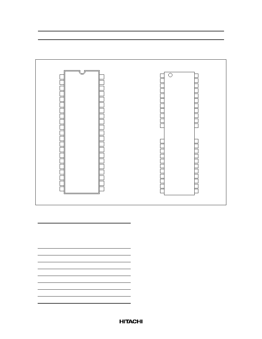
Pin Arrangement
1
2
3
4
5
6
7
8
9
10
11
15
16
17
18
19
20
21
22
23
24
25
50
49
48
47
46
45
44
43
42
41
40
36
35
34
33
32
31
30
29
28
27
26
CC
CC
CC
SS
SS
SS
V
I/O15
I/O14
I/O13
I/O12
V
I/O11
I/O10
I/O9
I/O8
NC
NC
LCAS
UCAS
OE
A9
A8
A7
A6
A5
A4
V
V
I/O0
I/O1
I/O2
I/O3
V
I/O4
I/O5
I/O6
I/O7
NC
NC
NC
WE
RAS
A11
A10
A0
A1
A2
A3
V
HM51W16165TT/LTT Series
(Top view)
1
2
3
4
5
6
7
8
9
10
11
12
13
14
15
16
17
18
19
20
21
42
41
40
39
38
37
36
35
34
33
32
31
30
29
28
27
26
25
24
23
22
V
I/O0
I/O1
I/O2
I/O3
V
I/O4
I/O5
I/O6
I/O7
NC
NC
WE
RAS
A11
A10
A0
A1
A2
A3
V
CC
CC
CC
V
I/O15
I/O14
I/O13
I/O12
V
I/O11
I/O10
I/O9
I/O8
NC
LCAS
UCAS
OE
A9
A8
A7
A6
A5
A4
V
SS
SS
SS
HM51W16165J/LJ Series
(Top view)
Pin Description
Pin name
Function
A0 to A11
Address input
·
Row/Refresh
address
·
Column address
A0 to A11
A0 to A7
I/O0 to I/O15
Data input/Data output
RAS
Row address strobe
UCAS, LCAS
Column address strobe
WE
Read/Write enable
OE
Output enable
V
CC
Power supply
V
SS
Ground
NC
No connection
This Material Copyrighted By Its Respective Manufacturer
HM51W16165 Series, HM51W18165 Series
4
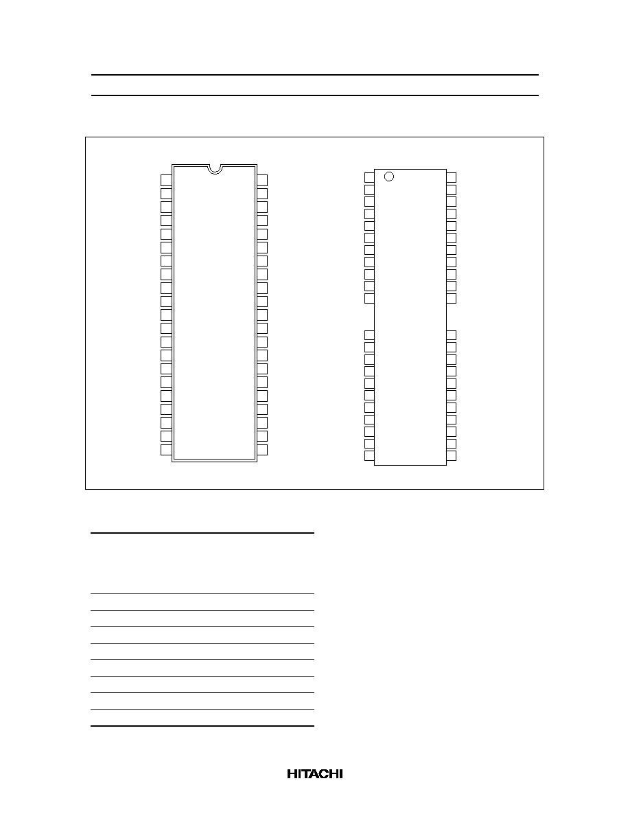
Pin Arrangement
V
I/O0
I/O1
I/O2
I/O3
V
I/O4
I/O5
I/O6
I/O7
NC
NC
WE
RAS
NC
NC
A0
A1
A2
A3
V
CC
CC
CC
V
I/O15
I/O14
I/O13
I/O12
V
I/O11
I/O10
I/O9
I/O8
NC
LCAS
UCAS
OE
A9
A8
A7
A6
A5
A4
V
SS
SS
SS
HM51W18165J/LJ Series
CC
CC
CC
SS
SS
SS
V
I/O15
I/O14
I/O13
I/O12
V
I/O11
I/O10
I/O9
I/O8
NC
NC
LCAS
UCAS
OE
A9
A8
A7
A6
A5
A4
V
V
I/O0
I/O1
I/O2
I/O3
V
I/O4
I/O5
I/O6
I/O7
NC
NC
NC
WE
RAS
NC
NC
A0
A1
A2
A3
V
HM51W18165TT/LTT Series
1
2
3
4
5
6
7
8
9
10
11
15
16
17
18
19
20
21
22
23
24
25
50
49
48
47
46
45
44
43
42
41
40
36
35
34
33
32
31
30
29
28
27
26
(Top view)
1
2
3
4
5
6
7
8
9
10
11
12
13
14
15
16
17
18
19
20
21
42
41
40
39
38
37
36
35
34
33
32
31
30
29
28
27
26
25
24
23
22
(Top view)
Pin Description
Pin name
Function
A0 to A9
Address input
·
Row/Refresh
address
·
Column address
A0 to A9
A0 to A9
I/O0 to I/O15
Data input/Data output
RAS
Row address strobe
UCAS
,
LCAS
Column address strobe
WE
Read/Write enable
OE
Output enable
V
CC
Power supply
V
SS
Ground
NC
No connection
This Material Copyrighted By Its Respective Manufacturer
HM51W16165 Series, HM51W18165 Series
5
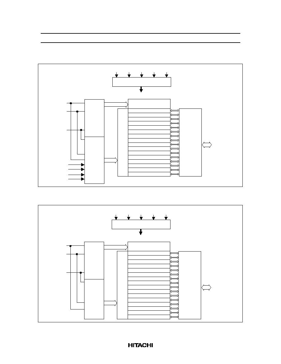
Block Diagram (HM51W16165 Series)
·
·
·
·
·
·
A0
A1
to
A7
A10
A11
A8
A9
Timing and control
RAS
UCAS LCAS
WE
OE
Column
address
buffers
Row
address
buffers
I/O buffers
I/O0
to
I/O15
Column decoder
Row decoder
1M array
1M array
1M array
1M array
1M array
1M array
1M array
1M array
1M array
1M array
1M array
1M array
1M array
1M array
1M array
1M array
Block Diagram(HM51W18165 Series)
·
·
·
·
·
·
A0
A1
to
A9
Timing and control
Column
address
buffers
Row
address
buffers
I/O buffers
I/O0
to
I/O15
Column decoder
Row decoder
1M array
1M array
1M array
1M array
1M array
1M array
1M array
1M array
1M array
1M array
1M array
1M array
1M array
1M array
1M array
1M array
RAS
UCAS LCAS
WE
OE
Truth Table
This Material Copyrighted By Its Respective Manufacturer