HM530281R Series
331,776-word
◊
8-bit Frame Memory
ADE-203-251B
Rev. 1.0
June 6, 1997
Description
The HM530281R series memory products provide completely asynchronous I/O and operate at the high
speed of 50 MHz. The HM530281R series memory products provide reset, jump, and line increment/hold
pointer control functions that can be used in synchronization with independent clocks on each of the I/O
ports. Memory can be accessed immediately without any waiting period after the execution of these
functions. In addition to the FIFO function, the 281R series products support an address structure that is
compatible with HDTV, NTSC, and PAL standards, and can be used in a wide range of applications, such
as noise reducers, TBC (time-based correction), inter-frame YC separation, and special function modes
(e.g., multi-freeze, P-in-P) in the digital TV, VCR, and video camera application. They are also appropriate
for use as inter-system speed conversion buffer memories in communications systems, as cache memories
of HDD and MOD, and as frame buffer of VGA.
Features
∑
Organization: 331,776-word
◊
8-bit
∑
Completely asynchronous operation of the serial read port and write port.
Internal generation of read and write addresses
Internal memory operation control provided on-chip
∑
High speed read/write cycle time: 50 MHz
∑
Reset, jump functions
Independent execution for read and write ports
Can be executed with arbitrary timing
Allow immediate access after execution (read/write) (for the jump function, when the address setup
is complete)
Jump address specifiable in 32-word units
∑
2 dimensional address
∑
Line increment/hold address pointer control function
∑
Window scan function

Datasheet Title
2
∑
Can handle HDTV, NTSC, and PAL standards
Line length: Up to 1152 bits (Arbitrary line lengths can also be handled by using the line reset
function.)
Line count: Up to 324 lines
∑
Built-in self-refresh eliminates the need for external refresh control.
∑
Power supply voltage: V
CC
= 5.0 V
±
10%.
Ordering Information
Type No.
Cycle Time
Memory Organization
Package
HM530281RTT-20
HM530281RTT-25
HM530281RTT-34
HM530281RTT-45
20 ns
25 ns
34 ns
45 ns
331,776 words
◊
8 bits
*2
1152 dots
◊
288 lines
◊
8 bits
*3
1024 dots
◊
324 lines
◊
8 bits
44-pin TSOP (TTP-44DB)
Notes: 1. Selectable following two kinds of addressing mode by mode pins
2. 1 dimensional addressing mode
3. 2 dimensional addressing mode
Pin Arrangement
1
2
3
4
5
6
7
8
9
10
11
12
13
14
15
16
17
18
19
20
21
22
44
43
42
41
40
39
38
37
36
35
34
33
32
31
30
29
28
27
26
25
24
23
Dout0
Dout1
Dout2
Dout3
Dout4
Dout5
Dout6
Dout7
V
V
OE
CGR
RCK
RRS
RLRS
RCLR
RWND
RAS
RAD
TEST1
TEST2
TEST3
Din0
Din1
Din2
Din3
Din4
Din5
Din6
Din7
V
V
WE
CGW
WCK
WRS
WLRS
WCLR
WWND
WAS
WAD
MODE0
MODE1
TEST0
SS
(Top view)
CC
SS
CC
Datasheet Title
4
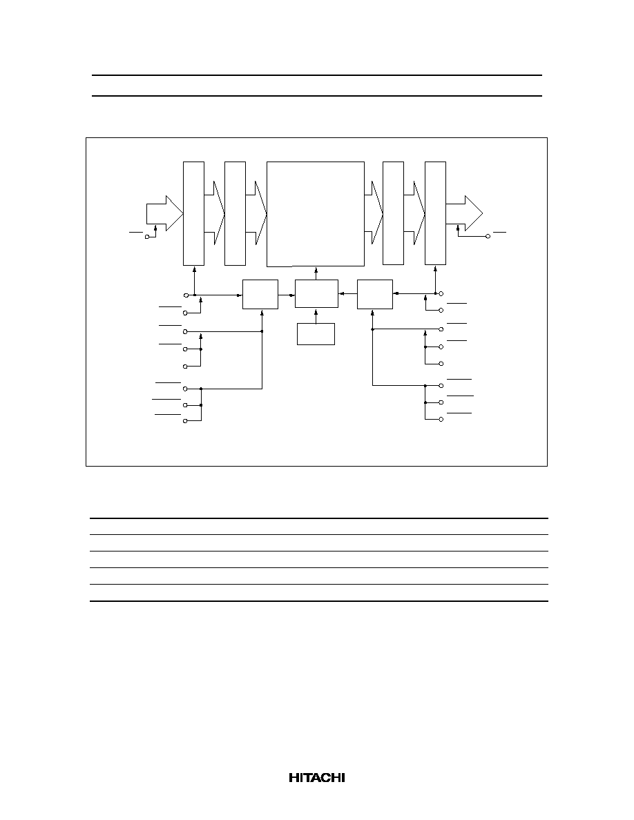
Block Diagram
Dout
OE
Write data register
Memory
array
1152 dot 288 line 8
1024 dot 324 line 8
10368 dot 32 word 8
◊
◊
◊
◊
◊
◊
*
*
*
Memory
controller
Write
counter
Read
counter
Din
WE
Refresh
counter
WCK
CGW
WRS
WAS
WAD
WLRS
WWND
WCLR
RCK
CGR
RRS
RAS
RAD
RLRS
RWND
RCLR
32-word
8
◊
32-word
8
◊
32-word
8
◊
32-word
8
◊
◊
8
1
1
1
◊
8
Write data buffer
Read data buffer
Read data register
Note : 1. Selected by the mode pin
Absolute Maximum Ratings
Parameter
Symbol
Value
Unit
Pin voltage
*1
V
T
≠1.0 to +7.0
V
Power dissipation
P
T
1.0
W
Operating temperature
Topr
0 to +70
∞
C
Storage temperature
Tstg
≠55 to +125
∞
C
Storage temperature (when biased)
Tbias
≠10 to +85
∞
C
Note:
1. The permissible values with respect to V
SS
.
Datasheet Title
5
Recommended DC Operating Conditions (Ta = 0 to +70
∞
C)
Parameter
Symbol
Min
Typ
Max
Unit
Power supply voltage
V
CC
4.5
5
5.5
V
V
SS
0
0
0
V
Input voltages
V
IH
2.7
--
6.5
V
V
IL
≠0.5
*1
--
0.6
V
Note:
1. When the pulse width is under 10 ns, V
IL
min = ≠3.0 V.
DC Characteristics (V
CC
= 5.0 V
±
10%, V
SS
= 0 V, Ta = 0 to +70
∞
C)
HM530281-20
HM530281-25
HM530281-34
HM530281-45
Test
Parameter Symbol Min Typ Max Min Typ Max Min Typ Max Min Typ Max Unit Conditions
Operating
power
supply
current
I
CCA
--
110 135 --
90
120 --
70
95
--
55
75
mA
Iout = 0,
t
WCC
= t
RCC
=
Min
Standby
power
supply
current
I
CCS
--
15
25
--
15
25
--
15
25
--
15
25
mA
V
CC
= 5.5 V
WCK, RCK =
"L" fix
Input
leakage
current
I
LI
≠10 --
10
≠10 --
10
≠10 --
10
≠10 --
10
mA
V
CC
= 5.5 V,
Vin = V
SS
to
V
CC
Output
leakage
current
I
LO
≠10 --
10
≠10 --
10
≠10 --
10
≠10 --
10
mA
OE = Vin
Vout = V
SS
to
V
CC
Output
voltages
V
OL
--
--
0.4
--
--
0.4
--
--
0.4
--
--
0.4
V
I
OL
= 2.1 mA
V
OH
2.4
--
--
2.4
--
--
2.4
--
--
2.4
--
--
V
I
OH
= ≠1.0 mA
Capacitance
*1
Parameter
Symbol
Typ
Max
Units
Test
Conditions
Input capacitance
Cin
--
5
pF
Vin = 0 V
Output capacitance
Cout
--
7
pF
Vout = 0 V
Note:
1. These parameters are sampled values, not values measured for all units.