Preliminary: The specification of this device are subject to change without notice. Please contact your nearest
Hitachi's Sales Dept. regarding specification.
HM621400HC Series
4M High Speed SRAM (4-Mword
◊
1-bit)
ADE-203-1199 (Z)
Preliminary
Rev. 0.0
Nov. 30, 2000
Description
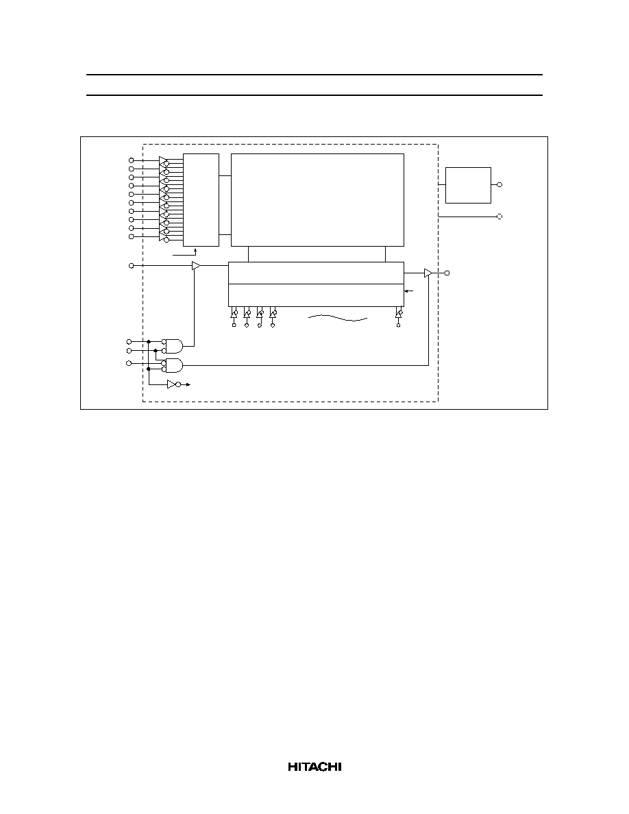
The HM621400HC is a 4-Mbit high speed static RAM organized 4-Mword
◊
1-bit. It has realized high speed
access time by employing CMOS process (6-transistor memory cell)and high speed circuit designing
technology. It is most appropriate for the application which requires high speed and high density memory,
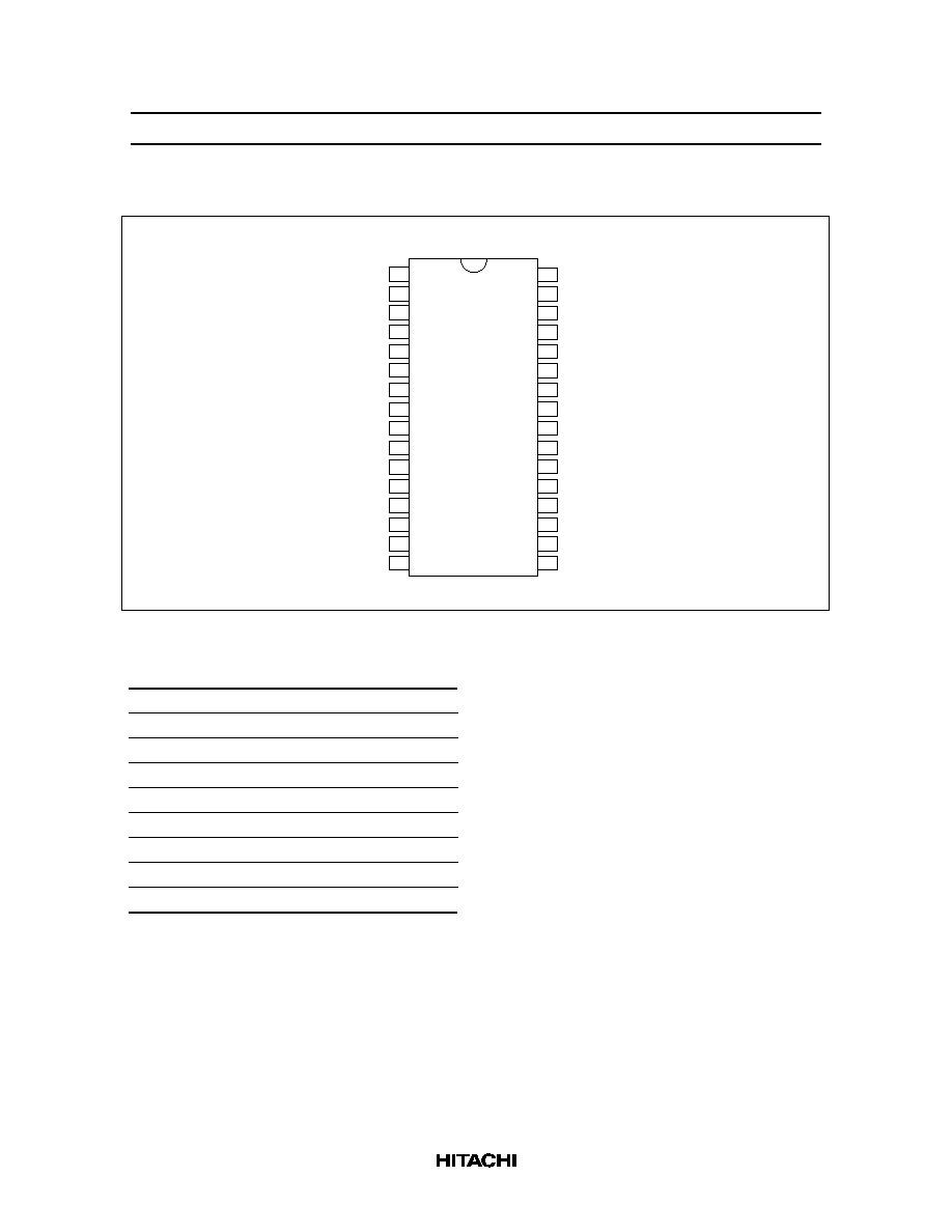
such as cache and buffer memory in system. The HM621400HC is packaged in 400-mil 32-pin SOJ for high
density surface mounting.
Features
∑
Single 5.0 V supply: 5.0 V ± 10 %
∑
Access time: 10 ns (max)
∑
Completely static memory
No clock or timing strobe required
∑
Equal access and cycle times
∑
Directly TTL compatible
All inputs and outputs
∑
Operating current: 140 mA (max)
∑
TTL standby current: 40 mA (max)
∑
CMOS standby current: 5 mA (max)
: 1.2 mA (max) (L-version)
∑
Data retension current: 0.8 mA (max) (L-version)
∑
Data retension voltage: 2 V (min) (L-version)
∑
Center V
CC
and V
SS
type pinout
HM621400HC Series
5
Operation Table
CS
OE
WE
Mode
V
CC
current
Dout
Ref. cycle
H
◊
◊
Standby
I
SB
, I
SB1
High-Z
--
L
H
H
Output disable
I
CC
High-Z
--
L
L
H
Read
I
CC
Dout
Read cycle (1) to (3)
L
H
L
Write
I
CC
High-Z
Write cycle (1)
L
L
L
Write
I
CC
High-Z
Write cycle (2)
Note:
◊
: H or L
Absolute Maximum Ratings
Parameter
Symbol
Value
Unit
Supply voltage relative to V
SS
V
CC
≠0.5 to +7.0
V
Voltage on any pin relative to V
SS
V
T
≠0.5*
1
to V
CC
+0.5*
2
V
Power dissipation
P
T
1.0
W
Operating temperature
Topr
0 to +70
∞C
Storage temperature
Tstg
≠55 to +125
∞C
Storage temperature under bias
Tbias
≠10 to +85
∞C
Notes: 1. V
T
(min) = ≠2.0 V for pulse width (under shoot) 6 ns.
2. V
T
(max) = V
CC
+ 2.0 V for pulse width (over shoot) 6 ns.
Recommended DC Operating Conditions (Ta = 0 to +70∞C)
Parameter
Symbol
Min
Typ
Max
Unit
Supply voltage
V
CC
*
3
4.5
5.0
5.5
V
V
SS
*
4
0
0
0
V
Input voltage
V
IH
2.2
--
V
CC
+ 0.5*
2
V
V
IL
≠0.5*
1
--
0.8
V
Notes: 1. V
IL
(min) = ≠2.0 V for pulse width (under shoot) 6 ns.
2. V
IH
(max) = V
CC
+ 2.0 V for pulse width (over shoot) 6 ns.
3. The supply voltage with all V
CC
pins must be on the same level.
4. The supply voltage with all V
SS
pins must be on the same level.