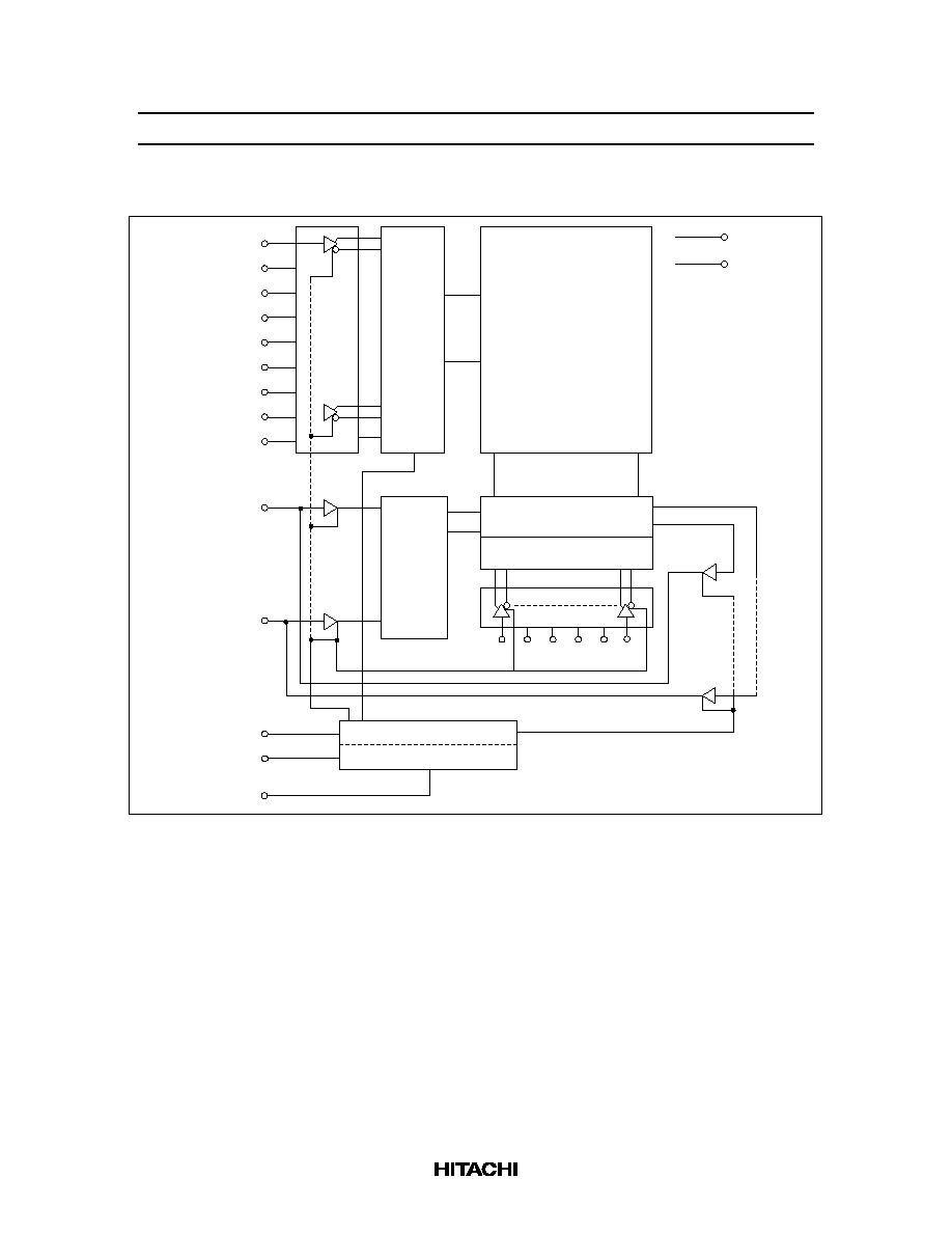
HM62256B Series
256k SRAM (32-kword
◊
8-bit)
ADE-203-135F (Z)
Rev. 6.0
Nov. 13, 1997
Description
The Hitachi HM62256B Series is a CMOS static RAM organized 32,768-word
◊
8-bit. It realizes higher
performance and low power consumption by employing 0.8
µ
m Hi-CMOS process technology. The
device, packaged in 8
◊
14 mm TSOP, 8
◊
13.4 mm TSOP with thickness of 1.2 mm, 450 mil SOP (foot
print pitch width), 600 mil plastic DIP, or 300 mil plastic DIP, is available for high density mounting. It
offers low power standby power dissipation; therefore, it is suitable for battery backup systems.
Features
∑
Single 5.0 V supply: 5.0 V
±
10%
∑
Access time: 55 ns/70 ns/85 ns (max)
∑
Power dissipation:
Active: 25 mW (typ) (f = 1 MHz)
Standby: 1.0
µ
W (typ)
∑
Completely static memory
No clock or timing strobe required
∑
Equal access and cycle times
∑
Common data input and output
Three state output
∑
Directly TTL compatible all inputs and outputs
∑
Battery backup operation
HM62256B Series
2
Ordering Information
Type No.
Access time
Package
HM62256BLP-7
70 ns
600-mil 28-pin plastic DIP (DP-28)
HM62256BLP-7SL
70 ns
HM62256BLSP-7
70 ns
300-mil 28-pin plastic DIP (DP-28NA)
HM62256BLSP-7SL
70 ns
HM62256BLFP-7T
70 ns
450-mil 28-pin plastic SOP (FP-28DA)
HM62256BLFP-5SLT
HM62256BLFP-7SLT
55 ns
70 ns
HM62256BLFP-7ULT
70 ns
HM62256BLT-8
85 ns
8 mm
◊
14 mm 32-pin TSOP (TFP-32DA)
HM62256BLT-7SL
70 ns
HM62256BLTM-8
85 ns
8 mm
◊
13.4 mm 28-pin TSOP (TFP-28DA)
HM62256BLTM-5SL
HM62256BLTM-7SL
55 ns
70 ns
HM62256BLTM-7UL
70 ns
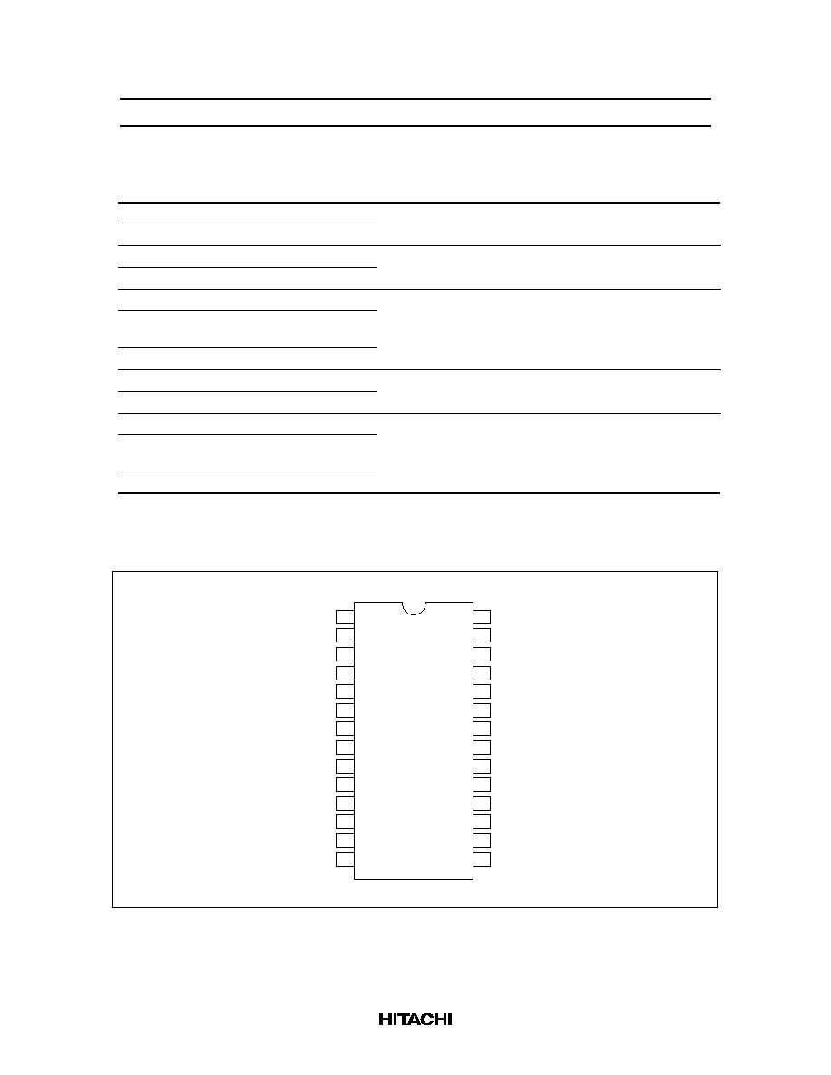
Pin Arrangement
1
2
3
4
5
6
7
8
9
10
11
12
13
14
28
27
26
25
24
23
22
21
20
19
18
17
16
15
A14
A12
A7
A6
A5
A4
A3
A2
A1
A0
I/O0
I/O1
I/O2
V
SS
V
CC
WE
A13
A8
A9
A11
OE
A10
CS
I/O7
I/O6
I/O5
I/O4
I/O3
HM62256BLP/BLFP/BLSP Series
(Top view)
HM62256B Series
3
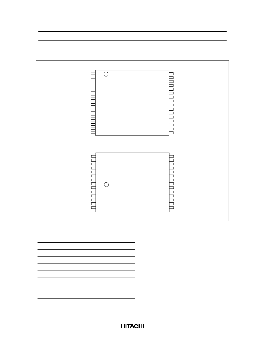
Pin Arrangement (cont.)
1
2
3
4
5
6
7
8
9
10
11
12
13
14
15
16
32
31
30
29
28
27
26
25
24
23
22
21
20
19
18
17
A10
CS
NC
I/O7
I/O6
I/O5
I/O4
I/O3
V
SS
I/O2
I/O1
I/O0
A0
NC
A1
A2
OE
A11
NC
A9
A8
A13
WE
V
CC
A14
A12
A7
A6
A5
NC
A4
A3
22
23
24
25
26
27
28
1
2
3
4
5
6
7
21
20
19
18
17
16
15
14
13
12
11
10
9
8
A10
CS
I/O7
I/O6
I/O5
I/O4
I/O3
V
SS
I/O2
I/O1
I/O0
A0
A1
A2
OE
A11
A9
A8
A13
WE
V
CC
A14
A12
A7
A6
A5
A4
A3
HM62256BLT Series
HM62256BLTM Series
(Top view)
(Top view)
Pin Description
Pin Name
Function
A0 to A14
Address input
I/O0 to I/O7
Data input/output
CS
Chip select
WE
Write enable
OE
Output enable
V
CC
Power supply
V
SS
Ground
NC
No connection

HM62256B Series
5
Operation Table
WE
CS
OE
Mode
V
CC
current
I/O pin
Ref. cycle
◊
H
◊
Standby
I
SB
, I
SB1
High-Z
--
H
L
H
Output disable
I
CC
High-Z
--
H
L
L
Read
I
CC
Dout
Read cycle (1)to (3)
L
L
H
Write
I
CC
Din
Write cycle (1)
L
L
L
Write
I
CC
Din
Write cycle (2)
Note:
◊
: H or L
Absolute Maximum Ratings
Parameter
Symbol
Value
Unit
Power supply voltage relative to V
SS
V
CC
≠0.5 to +7.0
V
Terminal voltage on any pin relative to V
SS
V
T
≠0.5*
1
to V
CC
+0.3*
2
V
Power dissipation
P
T
1.0
W
Operating temperature range
Topr
0 to +70
∞
C
Storage temperature range
Tstg
≠55 to +125
∞
C
Storage temperature range under bias
Tbias
≠10 to +85
∞
C
Notes: 1. V
T
min: ≠3.0 V for pulse half-width
50 ns
2. Maximum voltage is 7.0 V
DC Operating Conditions (Ta = 0 to +70
∞
C)
Parameter
Symbol
Min
Typ
Max
Unit
Notes
Supply voltage
V
CC
4.5
5.0
5.5
V
V
SS
0
0
0
V
Input high voltage
V
IH
2.2
--
V
CC
+ 0.3
V
Input low voltage
V
IL
≠0.5*
1
--
0.8
V
Note:
1. V
IL
min: ≠3.0 V for pulse half-width
50 ns