
HM628512BFP Series
4 M SRAM (512-kword
◊
8-bit)
ADE-203-1078B (Z)
Rev. 2.0
Nov. 23, 1999
Description
The Hitachi HM628512BFP is a 4-Mbit static RAM organized 512-kword
◊
8-bit. It realizes higher density,
higher performance and low power consumption by employing Hi-CMOS process technology. It is packaged
in standard 32-pin SOP.
Features
∑
Single 5 V supply
∑
Access time: 55/70 ns (max)
∑
Power dissipation
Active: 50 mW/MHz (typ)
Standby: 2 mW (max)
∑
Completely static memory. No clock or timing strobe required
∑
Equal access and cycle times
∑
Common data input and output: Three state output
∑
Directly TTL compatible: All inputs and outputs
Ordering Information
Type No.
Access time
Package
HM628512BFP-5
HM628512BFP-7
55 ns
70 ns
525-mil 32-pin plastic SOP (FP-32D)
HM628512BFP Series
2
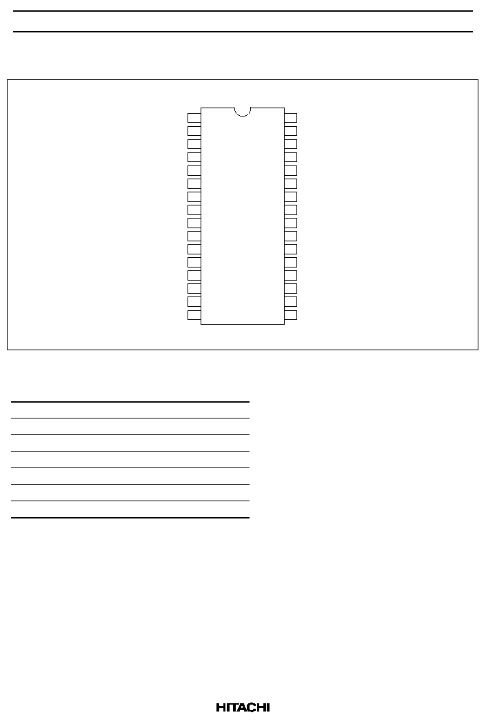
Pin Arrangement
1
2
3
4
5
6
7
8
9
10
11
12
13
14
15
16
32
31
30
29
28
27
26
25
24
23
22
21
20
19
18
17
A18
A16
A14
A12
A7
A6
A5
A4
A3
A2
A1
A0
I/O0
I/O1
I/O2
V
SS
V
A15
A17
WE
A13
A8
A9
A11
OE
A10
CS
I/O7
I/O6
I/O5
I/O4
I/O3
CC
(Top view)
32-pin SOP
Pin Description
Pin name
Function
A0 to A18
Address input
I/O0 to I/O7
Data input/output
CS
Chip select
OE
Output enable
WE
Write enable
V
CC
Power supply
V
SS
Ground
HM628512BFP Series
3
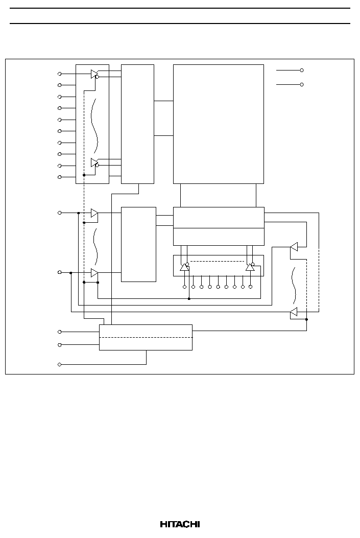
Block Diagram
∑
∑
∑
∑
∑
∑
∑
∑
∑
∑
∑
I/O0
I/O7
CS
WE
OE
A13 A17A15A8
A10
A11
V
V
CC
SS
Row
Decoder
Memory Matrix
1,024 4,096
Column I/O
Column Decoder
Input
Data
Control
◊
Timing Pulse Generator
Read/Write Control
A5
A9
A4
A18
A16
A1
A0
A2
A12
A14
A3
A7
A6
HM628512BFP Series
4
Function Table
WE
CS
OE
Mode
V
CC
current
Dout pin
Ref. cycle
◊
H
◊
Not selected
I
SB
, I
SB1
High-Z
--
H
L
H
Output disable
I
CC
High-Z
--
H
L
L
Read
I
CC
Dout
Read cycle
L
L
H
Write
I
CC
Din
Write cycle (1)
L
L
L
Write
I
CC
Din
Write cycle (2)
Note:
◊
: H or L
Absolute Maximum Ratings
Parameter
Symbol
Value
Unit
Power supply voltage
V
CC
≠0.5 to +7.0
V
Voltage on any pin relative to V
SS
V
T
≠0.5*
1
to V
CC
+ 0.3*
2
V
Power dissipation
P
T
1.0
W
Operating temperature
Topr
≠20 to +70
∞
C
Storage temperature
Tstg
≠55 to +125
∞
C
Storage temperature under bias
Tbias
≠20 to +85
∞
C
Notes: 1. ≠3.0 V for pulse half-width
30 ns
2. Maximum voltage is 7.0 V
Recommended DC Operating Conditions (Ta = ≠20 to +70
∞
C)
Parameter
Symbol
Min
Typ
Max
Unit
Supply voltage
V
CC
4.5
5.0
5.5
V
V
SS
0
0
0
V
Input high voltage
V
IH
2.2
--
V
CC
+ 0.3
V
Input low voltage
V
IL
≠0.3
*1
--
0.8
V
Note:
1. ≠3.0 V for pulse half-width
30 ns
HM628512BFP Series
5
DC Characteristics (Ta = ≠20 to +70
∞
C, V
CC
= 5 V
±
10% , V
SS
= 0 V)
Parameter
Symbol
Min
Typ*
1
Max
Unit
Test conditions
Input leakage current
|I
LI
|
--
--
1
µ
A
Vin = V
SS
to V
CC
Output leakage current
|I
LO
|
--
--
1
µ
A
CS
= V
IH
or
OE
= V
IH
or
WE
= V
IL
, V
I/O
= V
SS
to V
CC
Operating power supply current: DC
I
CC
--
8
15
mA
CS
= V
IL
,
others = V
IH
/V
IL
, I
I/O
= 0 mA
Operating power supply current
I
CC1
--
40
60
mA
Min cycle, duty = 100%
CS
= V
IL
, others = V
IH
/V
IL
I
I/O
= 0 mA
Operating power supply current
I
CC2
--
10
20
mA
Cycle time = 1
µ
s,
duty = 100%
I
I/O
= 0 mA,
CS
0.2 V
V
IH
V
CC
≠ 0.2 V, V
IL
0.2 V
Standby power supply current: DC
I
SB
--
1
3
mA
CS
= V
IH
Standby power supply current (1): DC I
SB1
--
300
400
µ
A
Vin
0 V,
CS
V
CC
≠ 0.2 V
Output low voltage
V
OL
--
--
0.4
V
I
OL
= 2.1 mA
Output high voltage
V
OH
2.4
--
--
V
I
OH
= ≠1.0 mA
Note:
1. Typical values are at V
CC
= 5.0 V, Ta = +25
∞
C and specified loading, and not guaranteed.
Capacitance (Ta = +25
∞
C, f = 1 MHz)
Parameter
Symbol
Typ
Max
Unit
Test conditions
Input capacitance*
1
Cin
--
8
pF
Vin = 0 V
Input/output capacitance*
1
C
I/O
--
10
pF
V
I/O
= 0 V
Note:
1. This parameter is sampled and not 100% tested.