Preliminary: The specification of this device are subject to change without notice. Please contact your
nearest Hitachi's Sales Dept. regarding specification.
HM628512CI Series
Wide Temperature Range Version
4 M SRAM (512-kword
◊
8-bit)
ADE-203-1211 (Z)
Preliminary
Rev. 0.0
Aug. 30, 2000
Description
The Hitachi HM628512CI is a 4-Mbit static RAM organized 512-kword
◊
8-bit. HM628512CI Series has
realized higher density, higher performance and low power consumption by employing Hi-CMOS process
technology. The HM628512CI Series offers low power standby power dissipation; therefore, it is suitable for
battery backup systems. It has packaged in 32-pin SOP, 32-pin TSOP II and 32-pin DIP.
Features
∑
Single 5 V supply
∑
Access time: 70 ns (max)
∑
Power dissipation
Active: 50 mW/MHz (typ)
Standby: 10
µ
W (typ)
∑
Completely static memory. No clock or timing strobe required
∑
Equal access and cycle times
∑
Common data input and output: Three state output
∑
Directly TTL compatible: All inputs and outputs
∑
Battery backup operation
∑
Operating temperature: ≠40 to +85∞C
HM628512CI Series
2
Ordering Information
Type No.
Access time
Package
HM628512CLPI-7
70 ns
600-mil 32-pin plastic DIP (DP-32)
HM628512CLFPI-7
70 ns
525-mil 32-pin plastic SOP (FP-32D)
HM628512CLTTI-7
70 ns
400-mil 32-pin plastic TSOP II (TTP-32D)
HM628512CLRRI-7
70 ns
400-mil 32-pin plastic TSOP II reverse (TTP-32DR)
HM628512CI Series
3
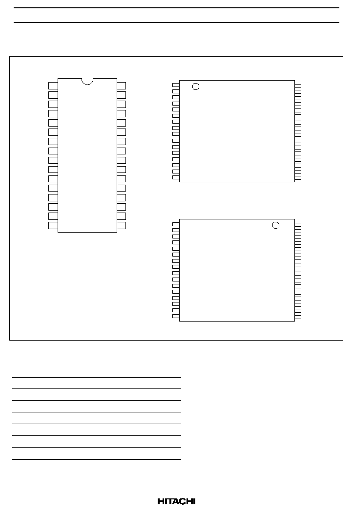
Pin Arrangement
1
2
3
4
5
6
7
8
9
10
11
12
13
14
15
16
32
31
30
29
28
27
26
25
24
23
22
21
20
19
18
17
SS
A18
A16
A14
A12
A7
A6
A5
A4
A3
A2
A1
A0
I/O0
I/O1
I/O2
V
V
A15
A17
WE
A13
A8
A9
A11
OE
A10
CS
I/O7
I/O6
I/O5
I/O4
I/O3
CC
32
31
30
29
28
27
26
25
24
23
22
21
20
19
18
17
1
2
3
4
5
6
7
8
9
10
11
12
13
14
15
16
SS
V
A15
A17
WE
A13
A8
A9
A11
OE
A10
CS
I/O7
I/O6
I/O5
I/O4
I/O3
A18
A16
A14
A12
A7
A6
A5
A4
A3
A2
A1
A0
I/O0
I/O1
I/O2
V
CC
1
2
3
4
5
6
7
8
9
10
11
12
13
14
15
16
32
31
30
29
28
27
26
25
24
23
22
21
20
19
18
17
A18
A16
A14
A12
A7
A6
A5
A4
A3
A2
A1
A0
I/O0
I/O1
I/O2
V
SS
V
A15
A17
WE
A13
A8
A9
A11
OE
A10
CS
I/O7
I/O6
I/O5
I/O4
I/O3
CC
(Top view)
32-pin DIP
32-pin SOP
32-pin TSOP
32-pin TSOP (reverse)
(Top view)
(Top view)
Pin Description
Pin name
Function
A0 to A18
Address input
I/O0 to I/O7
Data input/output
CS
Chip select
OE
Output enable
WE
Write enable
V
CC
Power supply
V
SS
Ground
HM628512CI Series
5
Function Table
WE
CS
OE
Mode
V
CC
current
Dout pin
Ref. cycle
◊
H
◊
Not selected
I
SB
, I
SB1
High-Z
--
H
L
H
Output disable
I
CC
High-Z
--
H
L
L
Read
I
CC
Dout
Read cycle
L
L
H
Write
I
CC
Din
Write cycle (1)
L
L
L
Write
I
CC
Din
Write cycle (2)
Note:
◊
: H or L
Absolute Maximum Ratings
Parameter
Symbol
Value
Unit
Power supply voltage
V
CC
≠0.5 to +7.0
V
Voltage on any pin relative to V
SS
V
T
≠0.5*
1
to V
CC
+ 0.3*
2
V
Power dissipation
P
T
1.0
W
Operating temperature
Topr
≠40 to +85
∞
C
Storage temperature
Tstg
≠55 to +125
∞
C
Storage temperature under bias
Tbias
≠40 to +85
∞
C
Notes: 1. V
T
min: ≠3.0 V for pulse half-width
30 ns.
2. Maximum voltage is 7.0 V.
Recommended DC Operating Conditions (Ta = ≠40 to +85
∞
C)
Parameter
Symbol
Min
Typ
Max
Unit
Supply voltage
V
CC
4.5
5.0
5.5
V
V
SS
0
0
0
V
Input high voltage
V
IH
2.4
--
V
CC
+ 0.3
V
Input low voltage
V
IL
≠0.3
*1
--
0.6
V
Note:
1. V
IL
min: ≠3.0 V for pulse half-width
30 ns.