
Preliminary: The specifications of this device are subject to change without notice. Please contact your
nearest Hitachi's Sales Dept. regarding specifications.
HM62G36256 Series
8M Synchronous Fast Static RAM
(256k-word
◊
36-bit)
ADE-203-1139 (Z)
Preliminary
Rev. 0.0
Jan. 10, 2000
Description
The HM62G36256 is a synchronous fast static RAM organized as 256-kword
◊
36-bit. It has realized high
speed access time by employing the most advanced CMOS process and high speed circuit designing
technology. It is most appropriate for the application which requires high speed, high density memory and
wide bit width configuration, such as cache and buffer memory in system. It is packaged in standard 119-
bump BGA.
Note:
All power supply and ground pins must be connected for proper operation of the device.
Features
∑
Power supply: 3.3 V +10%, ≠5%
∑
Clock frequency: 200 MHz to 250 MHz
∑
Internal self-timed late write
∑
Byte write control (4 byte write selects, one for each 9-bit)
∑
Optional
◊
18 configuration
∑
HSTL compatible I/O
∑
Programmable impedance output drivers
∑
User selective input trip-point
∑
Differential, HSTL clock inputs
∑
Asynchronous
G output control
∑
Asynchronous sleep mode
∑
Limited set of boundary scan JTAG IEEE 1149.1 compatible
∑
Protocol: Single clock register-register mode
HM62G36256 Series
2
Ordering Information
Type No.
Access time
Cycle time
Package
HM62G36256BP-4
HM62G36256BP-5
2.1 ns
2.5 ns
4.0 ns
5.0 ns
119-bump 1. 27 mm
14 mm
◊
22 mm BGA (BP-119A)
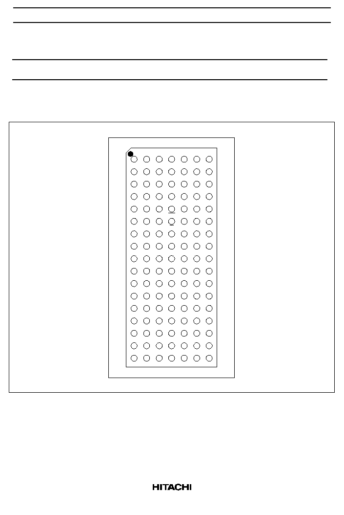
Pin Arrangement
1
2
3
4
5
6
7
A
B
C
D
E
F
G
H
J
K
L
M
N
P
R
T
U
VDDQ SA0
SA6
NC
SA4
SA2 VDDQ
NC
NC
SA7
NC
SA8
SA9
NC
NC SA14 SA3 VDD SA5
SA1
NC
DQc1 DQc0 VSS
ZQ
VSS DQb0 DQb1
DQc2 DQc3 VSS
SS
VSS DQb3 DQb2
VDDQ DQc4 VSS
G
VSS DQb4 VDDQ
DQc6 DQc5
SWEc
NC
DQb5 DQb6
DQc7 DQc8 VSS
NC
VSS DQb8 DQb7
VDDQ VDD VREF VDD VREF VDD VDDQ
DQd7 DQd8 VSS
K
VSS DQa8 DQa7
DQd6 DQd5
K SWEa
DQa5 DQa6
VDDQ DQd4 VSS
SWE
VSS DQa4 VDDQ
DQd2 DQd3 VSS SA17 VSS DQa3 DQa2
DQd1 DQd0 VSS SA16 VSS DQa0 DQa1
NC SA10 M1
VDD
M2 SA11 NC
NC
NC SA12 SA15 SA13 NC
ZZ
VDDQ TMS
TDI
TCK TDO
NC VDDQ
(Top view)
SWEb
SWEd
119-bumps BGA

HM62G36256 Series
3
Pin Description
Name
I/O type
Descriptions
Notes
V
DD
Supply
Core power supply
V
SS
Supply
Ground
V
DDQ
Supply
Output power supply
V
REF
Supply
Input reference: provides input reference voltage
K
Input
Clock input. Active high.
K
Input
Clock input. Active low.
SS
Input
Synchronous chip select
SWE
Input
Synchronous write enable
SAn
Input
Synchronous address input
n = 0, 1, 2...17
SWEx
Input
Synchronous byte write enables
x = a, b, c, d
G
Input
Asynchronous output enable
ZZ
Input
Power down mode select
ZQ
Input
Output impedance control
1
DQxn
I/O
Synchronous data input/output
x = a, b, c, d
n = 0, 1, 2...8
M1, M2
Input
Output protocol mode select
TMS
Input
Boundary scan test mode select
TCK
Input
Boundary scan test clock
TDI
Input
Boundary scan test data input
TDO
Output
Boundary scan test data output
NC
--
No connection
M1
M2
Protocol
Notes
V
SS
V
DD
Synchronous register to register operation
2
Notes: 1. ZQ is to be connected to V
SS
via a resistance RQ where 150
RQ
300
, if ZQ = V
DDQ
or
open, output buffer impedance will be maximum. A case of minimum impedance, it needs to
connect over 120
between ZQ and V
SS
.
2. There is 1 protocol with mode pin. Mode control pins (M1, M2) are to be tied either V
DD
or V
SS
respectively. The state of the Mode control inputs must be set before power-up and must not
change during device operation. Mode control inputs are not standard inputs and may not meet
V
IH
or V
IL
specification. This SRAM is tested only in the synchronous register to register
operation.

HM62G36256 Series
4
Block Diagram
A0 to A17
JTAG
register
JTAG
register
JTAG
register
JTAG
register
JTAG
register
JTAG
register
JTAG
register
JTAG
register
JTAG
register
JTAG tap
controller
R-Add
register
SS
register
SWE
register
SWEx
register
W-Add
register
SS
SWE
SWEx
G
ZZ
V
REF
ZQ
TDI
TCK
TMS
TDO
DQa0-8
DQb0-8
DQc0-8
DQd0-8
K
K
MUX
Row decoder
Multiplex
18
4
36
4
18
18
1
WRC
DOC
D-out
register
OB
D-in
register
WA
SA
Match
Column decoder
Memory
cell array
(256k
◊
36)
CLK
control
Impedance
contorol logic
HM62G36256 Series
5
Operation Table
ZZ
SS G
SWE SWEa SWEb SWEc SWEd
K
K
Operation
DQ (n)
DQ (n + 1)
H
◊
◊
◊
◊
◊
◊
◊
◊
◊
sleep mode
High-Z
High-Z
L
H
◊
◊
◊
◊
◊
◊
L-H H-L Dead
(not selected)
◊
High-Z
L
◊
H
◊
◊
◊
◊
◊
◊
◊
Dead
(Dummy read)
High-Z
High-Z
L
L
L
H
◊
◊
◊
◊
L-H H-L Read
◊
Dout
(a,b,c,d)0-8
L
L
◊
L
L
L
L
L
L-H H-L Write a, b, c, d
byte
High-Z
Din (a,b,c,d)0-8
L
L
◊
L
H
L
L
L
L-H H-L Write b, c, d
byte
High-Z
Din (b,c,d)0-8
L
L
◊
L
L
H
L
L
L-H H-L Write a, c, d
byte
High-Z
Din (a,c,d)0-8
L
L
◊
L
L
L
H
L
L-H H-L Write a, b, d
byte
High-Z
Din (a,b,d)0-8
L
L
◊
L
L
L
L
H
L-H H-L Write a, b, c
byte
High-Z
Din (a,b,c)0-8
L
L
◊
L
H
H
L
L
L-H H-L Write c, d byte High-Z
Din (c,d)0-8
L
L
◊
L
L
H
H
L
L-H H-L Write a, d byte High-Z
Din (a,d)0-8
L
L
◊
L
L
L
H
H
L-H H-L Write a, b byte High-Z
Din (a,b)0-8
L
L
◊
L
H
L
L
H
L-H H-L Write b, c byte High-Z
Din (b,c)0-8
L
L
◊
L
H
H
H
L
L-H H-L Write d byte
High-Z
Din (d)0-8
L
L
◊
L
H
H
L
H
L-H H-L Write c byte
High-Z
Din (c)0-8
L
L
◊
L
H
L
H
H
L-H H-L Write b byte
High-Z
Din (b)0-8
L
L
◊
L
L
H
H
H
L-H H-L Write a byte
High-Z
Din (a)0-8
Notes: 1.
◊
means don't care for synchronous inputs, and H or L for asynchronous inputs.
2.
SWE
,
SS
,
SWEa
to
SWEd
, SA are sampled at the rising edge of K clock.
3. Although differential clock operation is implied, this SRAM will operate properly with one clock
phase (either K or
K
) tied to V
REF
. Under such single-ended clock operation, all parameters
specified within this document will be met.