Rev.2.00, Oct.06.2003, page 1 of 23
HM62V16100I Series
Wide Temperature Range Version
16 M SRAM (1-Mword
◊
16-bit)
REJ03C0060-0200Z
Rev. 2.00
Oct.06.2003
Description
The HM62V16100I Series is 16-Mbit static RAM organized 1-Mword
◊
16-bit. HM62V16100I Series has
realized higher density, higher performance and low power consumption by employing CMOS process
technology (6-transistor memory cell). It offers low power standby power dissipation; therefore, it is
suitable for battery backup systems. It has the package variations of 48-bump chip size package with 0.75
mm bump pitch and 48-pin plastic TSOPI for high density surface mounting.
Features
∑
Single 3.0 V supply: 2.7 V to 3.6 V
∑
Fast access time: 45/55 ns (max)
∑
Power dissipation:
Active: 9 mW/MHz (typ)
Standby: 1.5
µ
W (typ)
∑
Completely static memory.
No clock or timing strobe required
∑
Equal access and cycle times
∑
Common data input and output.
Three state output
∑
Battery backup operation.
2 chip selection for battery backup
∑
Temperature range:
-
40 to +85
∞
C
HM62V16100I Series
Rev.2.00, Oct.06.2003, page 2 of 23
Ordering Information
Type No.
Access time
Package
HM62V16100LTI-4
45 ns
48-pin plastic TSOPI (normal-bend type) (TFP-48DA)
HM62V16100LTI-4SL 45
ns
HM62V16100LTI-5SL 55
ns
HM62V16100LBPI-4
45 ns
48-bump CSP with 0.75 mm bump pitch (TBP-48F)
HM62V16100LBPI-4SL 45
ns
HM62V16100LBPI-5SL 55
ns
HM62V16100I Series
Rev.2.00, Oct.06.2003, page 4 of 23
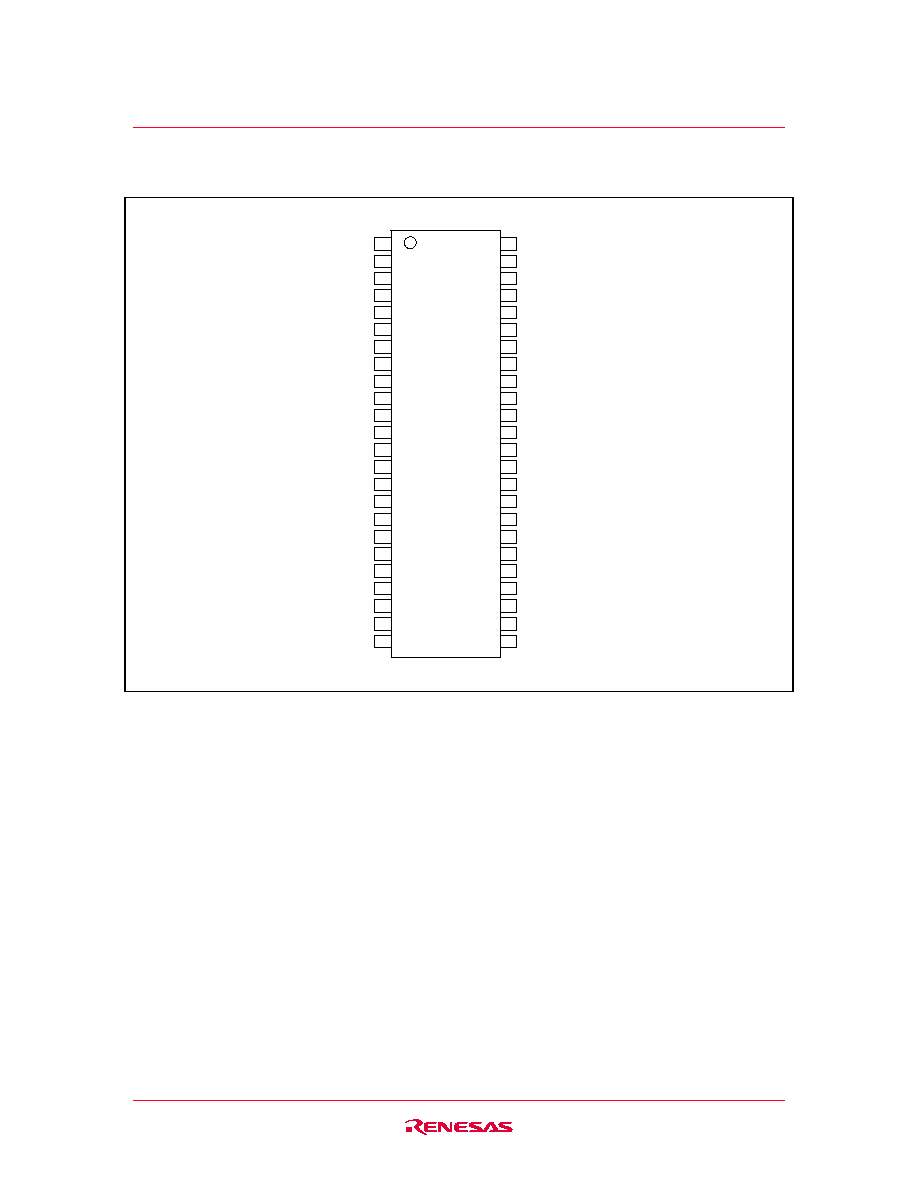
Pin Description (TSOP)
Pin name
Function
A0 to A19
Address input (word mode)
A-1 to A19
Address input (byte mode)
I/O0 to I/O15
Data input/output
CS1
Chip select 1
CS2
Chip select 2
WE
Write
enable
OE
Output
enable
LB
Lower byte select
UB
Upper byte select
BYTE
Byte
enable
V
CC
Power
supply
V
SS
Ground
NC No
connection
NU*
1
Not used (test mode pin)
Note: 1. This pin should be connected to a ground (V
SS
), or not be connected (open).
HM62V16100I Series
Rev.2.00, Oct.06.2003, page 5 of 23
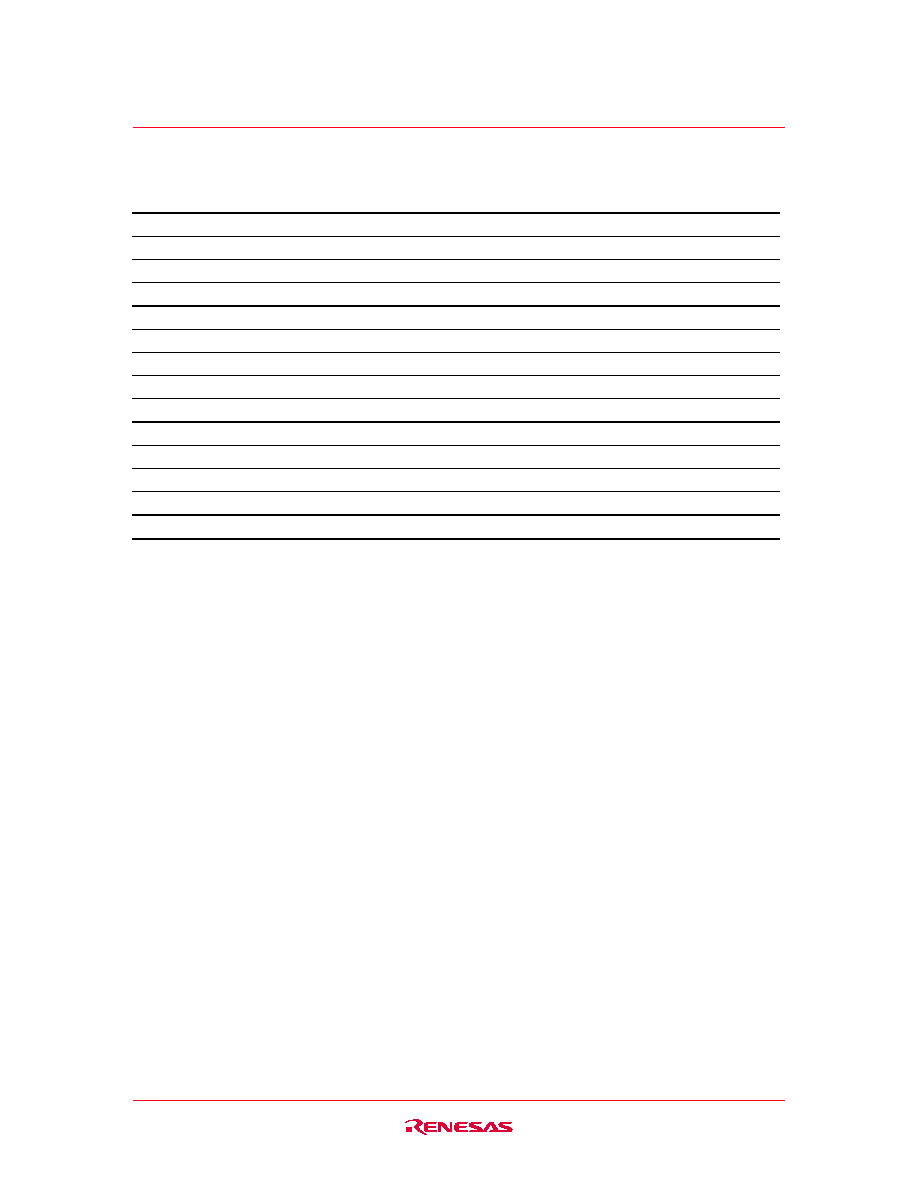
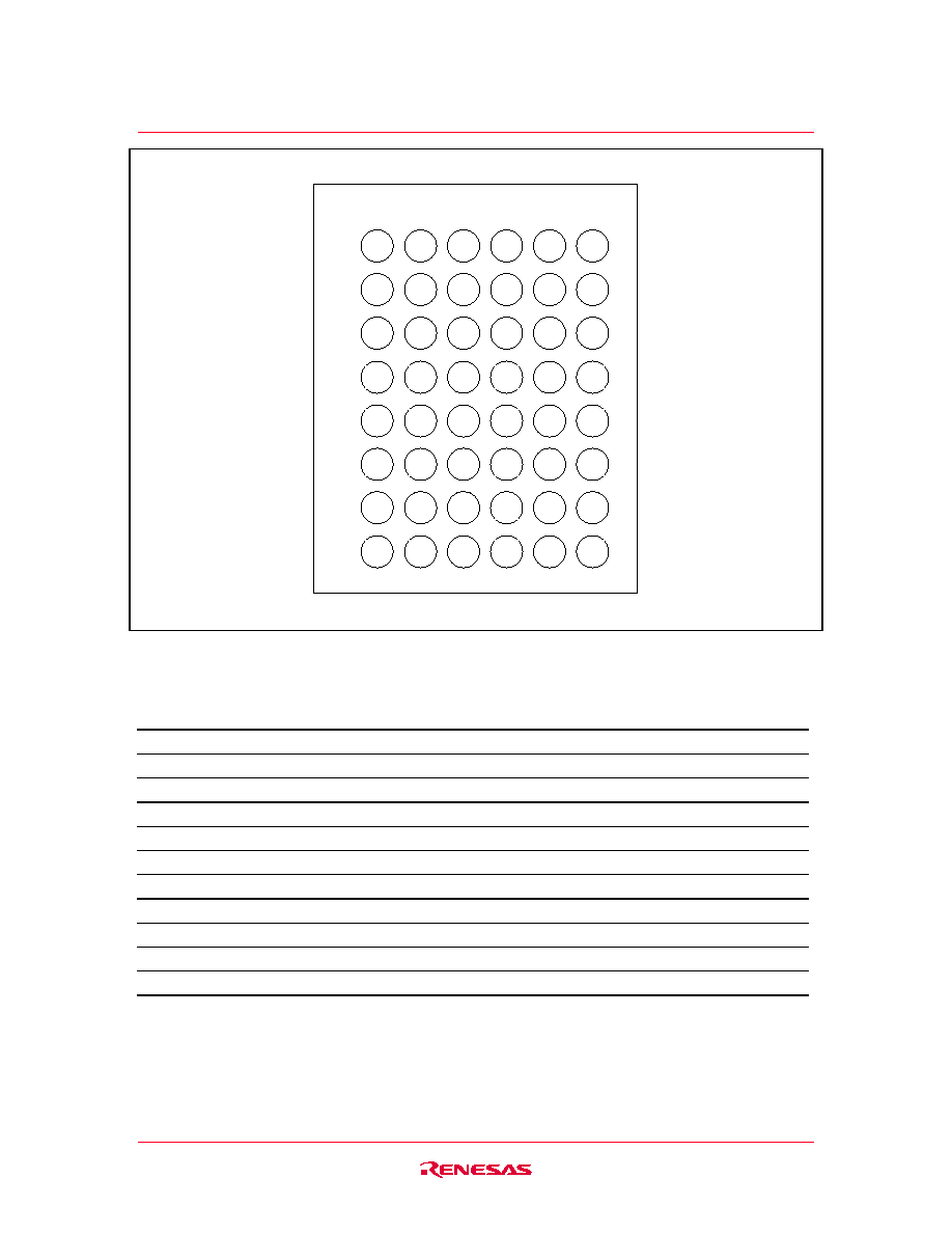
(Top view)
48-bumps CSP
A
B
C
D
E
F
G
H
1 2 3 4 5 6
LB
I/O8
I/O9
VSS
VCC
I/O14
I/O15
A18
OE
UB
I/O10
I/O11
I/O12
I/O13
A19
A8
A3
A5
A17
VSS
A14
A0
A12
A9
A1
A4
A6
A7
A16
A15
A13
A10
A2
CS1
I/O1
I/O3
I/O4
I/O5
WE
A11
CS2
I/O0
I/O2
VCC
VSS
I/O6
I/O7
NU
Pin Description (CSP)
Pin name
Function
A0 to A19
Address input
I/O0 to I/O15
Data input/output
CS1
Chip select 1
CS2
Chip select 2
WE
Write
enable
OE
Output
enable
LB
Lower byte select
UB
Upper byte select
V
CC
Power
supply
V
SS
Ground
NU*
1
Not used (test mode pin)
Note: 1. This pin should be connected to a ground (V
SS
), or not be connected (open).