 | –≠–ª–µ–∫—Ç—Ä–æ–Ω–Ω—ã–π –∫–æ–º–ø–æ–Ω–µ–Ω—Ç: HN58C65 | –°–∫–∞—á–∞—Ç—å:  PDF PDF  ZIP ZIP |
HN58C65 Series
8192-word
◊
8-bit Electrically Erasable and Programmable CMOS
ROM
ADE-203-374A (Z)
Rev. 1.0
Apr. 12, 1995
Description
The Hitachi HN58C65 is a electrically erasable and programmable ROM organized as 8192-word
◊
8-bit. It
realizes high speed, low power consumption, and a high level of reliability, employing advanced MNOS
memory technology and CMOS process and circuitry technology. It also has a 32-byte page programming
function to make its erase and write operations faster.
Features
∑
Single 5 V Supply
∑
On chip latches: address, data, CE, OE, WE
∑
Automatic byte write: 10 ms max
∑
Automatic page write (32 byte): 10 ms max
∑
Fast access time: 250 ns max
∑
Low power dissipation: 20 mW/MHz typ (Active)
2.0 mW typ (Standby)
∑
Data polling and Ready/Busy
∑
Data protection circuity on power on/power off
∑
Conforms to JEDEC byte-wide standard
∑
Reliable CMOS with MNOS cell technology
∑
10
5
erase/write cycles (in page mode)
∑
10 year data retention
Ordering Information
Type No.
Access Time
Package
HN58C65P-25
250 ns
600 mil 28 pin plastic DIP (DP-28)
HN58C65FP-25
250 ns
28 pin plastic SOP
*1
(FP-28D/DA)
Note:
1. T is added to the end of the type no. for a SOP of 3.0 mm (max) thickness.
HN58C65 Series
2
Pin Arrangement
1
2
3
4
5
6
7
8
9
10
11
12
13
14
28
27
26
25
24
23
22
21
20
19
18
17
16
15
V
WE
NC
A8
A9
A11
OE
A10
CE
I/O7
I/O6
I/O5
I/O4
I/O3
RDY/Busy
A12
A7
A6
A5
A4
A3
A2
A1
A0
I/O0
I/O1
I/O2
V
SS
CC
(Top View)
HN58C65P/FP Series
Pin Description
Pin Name
Function
A0 ≠ A12
Address input
I/O1 ≠ I/O7
Data input/output
OE
Output enable
CE
Chip enable
WE
Write enable
V
CC
Power (+5 V)
V
SS
Ground
NC
No connection
RDY/
Busy
Ready/
Busy
HN58C65 Series
3
Block Diagram
V
V
OE
CE
A4
A0
A5
A12
WE
CC
SS
I/O0
I/O7
High Voltage Generator
Control Logic and Timing
Y Decoder
X Decoder
Address
Buffer and
Latch
I/O Buffer
and
Input Latch
Y Gating
Memory Array
Data Latch
RDY/Busy
Mode Selection
Pin Mode
CE
OE
WE
RDY/
Busy
I/O
Read
V
IL
V
IL
V
IH
High-Z
Dout
Standby
V
IH
X
*1
X
High-Z
High-Z
Write
V
IL
V
IH
V
IL
High-Z to V
OL
Din
Deselect
V
IL
V
IH
V
IH
High-Z
High-Z
Write inhibit
X
X
V
IH
X
V
IL
X
High-Z
--
Data
polling
V
IL
V
IL
V
IH
V
OL
Data out (I/O7)
Note:
1. X = Don't care

HN58C65 Series
4
Absolute Maximum Ratings
Parameter
Symbol
Value
Unit
Supply voltage
*1
V
CC
≠0.6 to +7.0
V
Input voltage
*1
Vin
≠0.5
*2
to +7.0
V
Operating temperature range
*3
Topr
0 to +70
∞
C
Storage temperature range
Tstg
≠55 to +125
∞
C
Notes: 1. With respect to V
SS
2. ≠3.0 V for pulse width
50 ns.
3. Including electrical characteristics and data retention.
Recommended DC Operating Conditions
Parameter
Symbol
Min
Typ
Max
Unit
Supply voltage
V
CC
4.5
5.0
5.5
V
Input voltage
V
IL
≠0.3
--
0.8
V
V
IH
2.2
--
V
CC
+ 1
V
Operating temperature
Topr
0
--
70
∞
C

HN58C65 Series
5
DC Characteristics (Ta = 0 to +70
∞
C, V
CC
= 5 V
±
10%)
Parameter
Symbol
Min
Typ
Max
Unit
Test Conditions
Input leakage current
I
LI
--
--
2
µ
A
V
CC
= 5.5 V
Vin = 5.5 V
Output leakage current
I
LO
--
--
2
µ
A
V
CC
= 5.5 V
Vout = 5.5/0.4 V
V
CC
current (Standby)
I
CC1
--
--
1
mA
CE
= V
IH
,
CE
= V
CC
V
CC
current (Active)
I
CC2
--
--
8
mA
Iout = 0 mA
Duty = 100%
Cycle = 1
µ
s at
V
CC
= 5.5 V
--
--
25
mA
Iout = 0 mA
Duty = 100%
Cycle = 250 ns at
V
CC
= 5.5 V
Input low voltage
V
IL
≠0.3
*1
--
0.8
V
Input high voltage
V
IH
2.2
--
V
CC
+ 1
V
Output low voltage
V
OL
--
--
0.4
V
I
OL
= 2.1 mA
Output high voltage
V
OH
2.4
--
--
V
I
OH
= ≠400
µ
A
Note:
1. ≠1.0 V for pulse width
50 ns
Capacitance (Ta = 25
∞
C, f = 1 MHz)
Parameter
Symbol
Min
Typ
Max
Unit
Test Conditions
Input capacitance
*1
Cin
--
--
6
pF
Vin = 0 V
Output capacitance
*1
Cout
--
--
12
pF
Vout = 0 V
Note:
1. This parameter is periodically sampled and not 100% tested.
AC Characteristics (Ta = 0 to +70
∞
C, V
CC
= 5 V
±
10%)
Test Conditions
∑
Input pulse levels: 0.4 V to 2.4 V
∑
Input rise and fall time:
20 ns
∑
Output load: 1TTL gate + 100 pF
∑
Reference levels for measuring timing: 0.8 V and 2 V
HN58C65 Series
6
Read Cycle
Parameter
Symbol
Min
Max
Unit
Test Conditions
Address to output delay
t
ACC
--
250
ns
CE
=
OE
= V
IL
,
WE
= V
IH
CE
to output delay
t
CE
--
250
ns
OE
= V
IL
,
WE
= V
IH
OE
to output delay
t
OE
10
100
ns
CE
= V
IL
,
WE
= V
IH
Address to output hold
t
OH
0
--
ns
CE
=
OE
= V
IL
,
WE
= V
IH
OE, CE
high to output float
*1
t
DF
0
90
ns
CE
= V
IL
,
WE
= V
IH
Note:
1. t
DF
is defined at which the outputs archieve the open circuit conditions and are no longer driven.
Read Timing Waveform
Address
CE
OE
WE
Data Out
High
Data Out Valid
t
ACC
t
CE
t
OE
t
OH
t
DF

HN58C65 Series
7
Write Cycle
Parameter
Symbol
Min
*1
Typ
Max
Unit
Test Conditions
Address setup time
t
AS
0
--
--
ns
Address hold time
t
AH
150
--
--
ns
CE
to write setup time (
WE
controlled)
t
CS
0
--
--
ns
CE
hold time (
WE
controlled)
t
CH
0
--
--
ns
WE
to write setup time (
CE
controlled)
t
WS
0
--
--
ns
WE
hold time (
CE
controlled)
t
WH
0
--
--
ns
OE
to write setup time
t
OES
0
--
--
ns
OE
hold time
t
OEH
0
--
--
ns
Data setup time
t
DS
100
--
--
ns
Data hold time
t
DH
20
--
--
ns
WE
pulse width (
WE
controlled)
t
WP
200
--
--
ns
CE
pulse width (
CE
controlled)
t
CW
200
--
--
ns
Data latch time
t
DL
100
--
--
ns
Byte lode cycle
t
BLC
0.30
--
30
µ
s
Byte lode window
t
BL
100
--
--
µ
s
Write cycle time
t
WC
--
--
10
*2
ms
Time to devce busy
t
DB
120
--
--
ns
Write start time
t
DW
150
--
--
ns
Notes: 1. Use this device in longer cycle than this value.
2. t
WC
must be longer than this value unless polling technique is used. This device automatically
completes the internal write operation within this value.

HN58C65 Series
8
Byte Write Timing Waveform (1) (WE Controlled)
Address
CE
WE
OE
Din
RDY/Busy
t
WC
t
CH
t
AH
t
CS
t
AS
t
WP
t
OEH
t
BL
t
OES
t
DS
t
DH
t
DB
High-Z
High-Z
t
DW
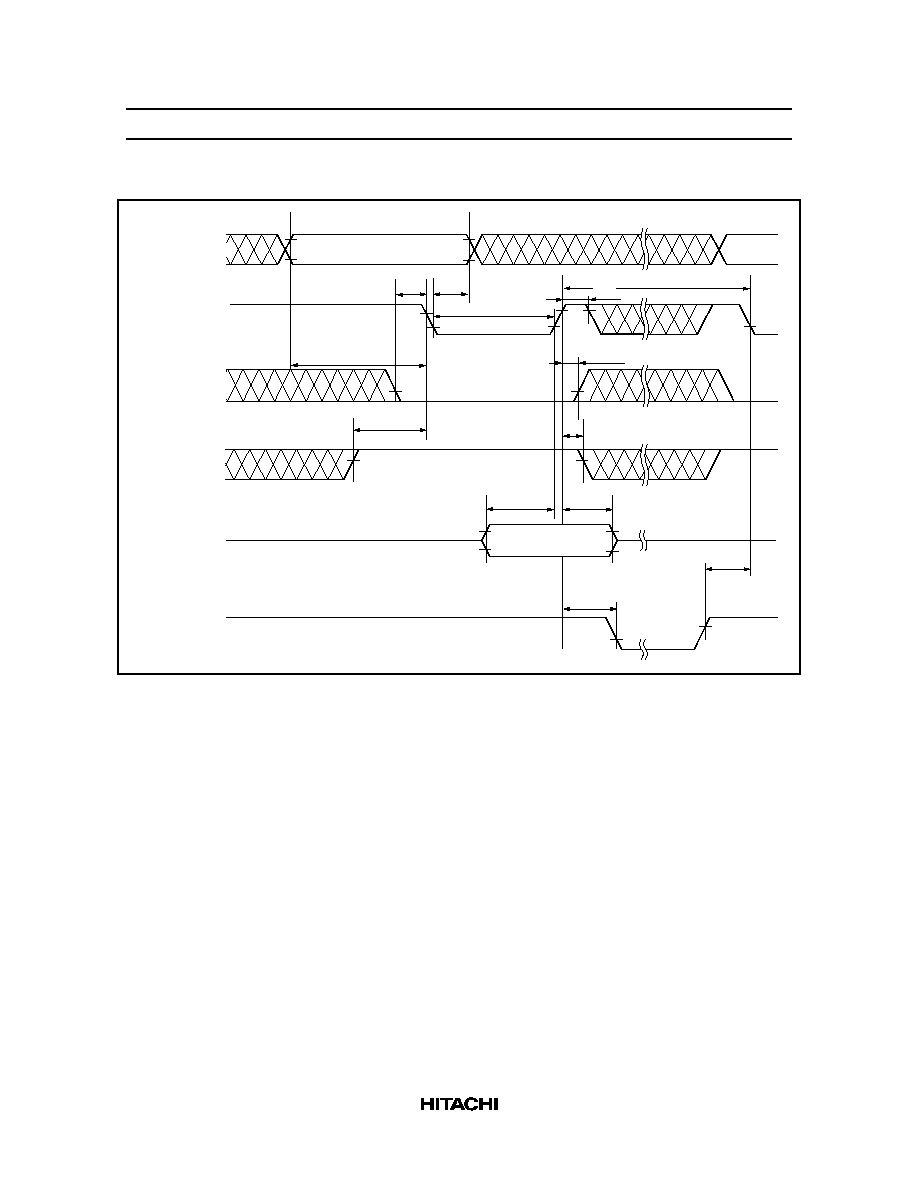
HN58C65 Series
9
Byte Write Timing Waveform (2) (CE Controlled)
Address
CE
WE
OE
Din
RDY/
Busy
t
WC
t
AH
t
WS
t
AS
t
OEH
t
WH
t
OES
t
DS
t
DH
t
DB
t
CW
t
BL
t
DW
High-Z
High-Z

HN58C65 Series
10
Page Write Timing Waveform (1) (WE Controlled)
Address
A0 to A4
WE
CE
OE
Din
RDY/
Busy
t
AS
t
AH
t
BL
t
WC
t
OEH
t
DH
t
DB
t
OES
t
CH
t
CS
WP
t
DL
t
BLC
t
t
DS
t
DW
High-Z
High-Z
Address
A5 to A12
HN58C65 Series
11
Page Write Timing Waveform (2) (CE Controlled)
Address
A0 to A4
WE
CE
OE
Din
RDY/
Busy
t
AS
t
AH
t
BL
t
WC
t
OEH
t
DH
t
DB
t
OES
t
WH
t
WS
CW
t
DL
t
BLC
t
t
DS
t
DW
High-Z
High-Z
Address
A5 to A12

HN58C65 Series
12
Data Polling Timing Waveform
t
BL
t
WC
t
DW
t
OES
Address
CE
WE
OE
I/O7
t
OE
Din X
An
An
Dout
X
Dout X
An
Functional Description
Automatic Page Write
Page-mode write feature allows 1 to 32 bytes of data to be written into the EEPROM in a single write cycle.
Following the initial byte cycle, an additional 1 to 31 bytes can be written in the same manner. Each
additional byte load cycle must be started within 30
µ
s of the preceding rising edge of the WE. When CE or
WE is high for 100
µ
s after data input, the EEPROM enters write mode automatically and the input data are
written into the EEPROM.
Data Polling
Data polling allows the status of the EEPROM to be determined. If EEPROM is set to read mode during a
write cycle, an inversion of the last byte of data to be loaded outputs from I/O7 to indicate that the EEPROM
is performing a write operation.
RDY/Busy Signal
RDY/Busy signal also allows the status of the EEPROM to be determined. The RDY/Busy signal has high
impedance, except in write cycle and is lowered to V
OL
after the first write signal. At the end of a write cycle,
the RDY/Busy signal changes state to high impedance.

HN58C65 Series
13
WE, CE Pin Operation
During a write cycle, addresses are latched by the falling edge of WE or CE and data is latched by the rising
edge of WE or CE.
Write/Erase Endurance and Data Retention Time
The endurance is 10
5
cycles in case of the page programming and 3
◊
10
3
cycles in case of byte programming
(1% cumulative failure rate). The data retention time is more than 10 years when a device is page-
programmed less than 10
4
cycles.
Data Protection
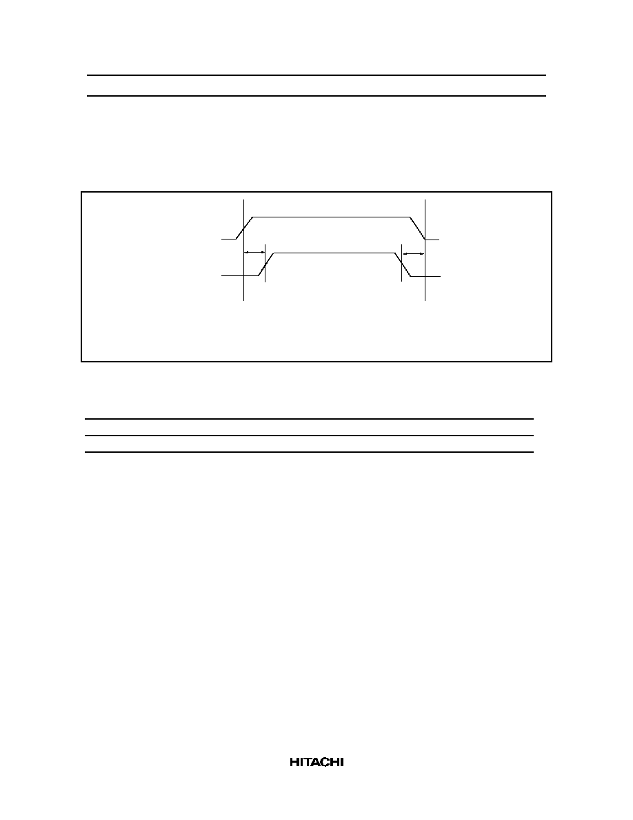
1. Data Protection against Noise on Control Pins (CE, OE, WE) during Operation
During readout or standby, noise on the control pins may act as a trigger and turn the EEPROM to progam
mode by mistake. To prevent this phenomenon, this device has a noise cancelation function that cuts
noise if its width is 20 ns or less in program mode. Be careful not to allow noise of a width of more than
20 ns on the control pins.
WE
CE
OE
5 V
0 V
5 V
0 V
20 ns max
HN58C65 Series
14
2. Data Protection at V
CC
On/Off
When V
CC
is turned on or off, noise on the control pins generated by external circuits (CPU, etc.) may act
as a trigger and turn the EEPROM to program mode by mistake. To prevent this unintentional
programming, the EEPROM must be kept in an unprogrammable state while the CPU is in an unstable
state.
V
CC
CPU
RESET
Unprogrammable
Unprogrammable
*
*
*The EEPROM should be kept in unprogrammable
state during V
CC
on/off by using CPU RESET signal.
In addition, when V
CC
is turned on or off, the input level of on control pins must be held as shown in the
table below.
CE
V
CC
X
X
OE
X
V
SS
X
WE
X
X
V
CC
X: Don't care.
V
CC
: Pull-up to V
CC
level
V
SS
: Pull-down to V
SS
level.

HN58C65 Series
15
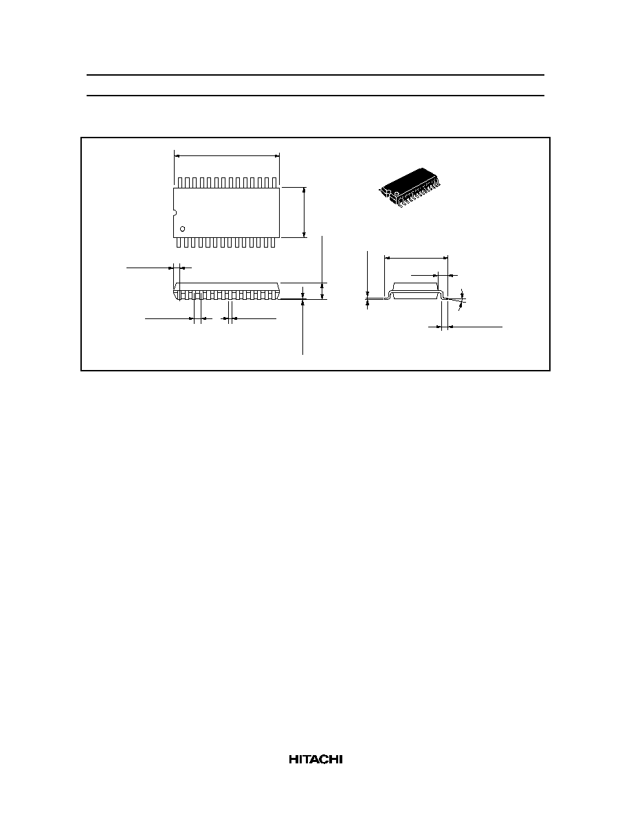
Package Dimensions
HN58C65P series (DP-28)
Unit: mm
0.51 Min
2.54 Min
0.25
+ 0.11
≠ 0.05
2.54 ± 0.25
0.48 ± 0.10
0∞ ≠ 15∞
15.24
1.20
35.60
36.50 Max
13.40
14.60 Max
1
14
15
28
5.70 Max
1.90 Max
HN58C65FP Series (FP-28D)
Unit: mm
0 ≠ 10 ∞
+ 0.08
≠ 0.07
0.17
1.00 ± 0.20
0.20 ± 0.10
2.50 Max
1.27
0.40
+ 0.10
≠ 0.05
8.40
18.30
18.75 Max
1.12 Max
28
15
1
14
11.80 ± 0.30
0.20
M
0.15
1.70
HN58C65 Series
16
HN58C65FP Series (FP-28DA)
Unit: mm
+ 0.08
≠ 0.07
0.17
0.20 ± 0.10
3.00 Max
1.27 ± 0.10
0.40
+ 0.10
≠ 0.05
8.40
18.00
18.75 Max
1.27 Max
28
15
1
14
11.80 ± 0.30
0 ≠ 10 ∞
1.00 ± 0.20
1.70