Document Outline
- D e s c r i p t i o n
- F e a t u r e s
- O r d e r i n g I n f o r m a t i o n
- P i n A r r a n g e m e n t
- P i n D e s c r i p t i o n
- B l o c k D i a g r a m
- O p e r a t i o n T a b l e
- A b s o l u t e M a x i m u m R a t i n g s
- R e c o m m e n d e d D C O p e r a t i n g C o n d i t i o n s
- D C C h a r a c t e r i s t i c s
- C a p a c i t a n c e
- A C C h a r a c t e r i s t i c s
- T i m i n g W a v e f o r m s
- R e a d T i m i n g W a v e f o r m
- B y t e W r i t e T i m i n g W a v e f o r m ( 1 ) ( W E C o n t r o l l e d )
- B y t e W r i t e T i m i n g W a v e f o r m ( 2 ) ( C E C o n t r o l l e d )
- P a g e W r i t e T i m i n g W a v e f o r m ( 1 ) ( W E C o n t r o l l e d )
- P a g e W r i t e T i m i n g W a v e f o r m ( 2 ) ( C E C o n t r o l l e d )
- D a t a P o l l i n g T i m i n g W a v e f o r m
- T o g g l e b i t W a v e f o r m
- S o f t w a r e D a t a P r o t e c t i o n T i m i n g W a v e f o r m ( 1 ) ( i n p r o t e c t i o n m o d
- S o f t w a r e D a t a P r o t e c t i o n T i m i n g W a v e f o r m ( 2 ) ( i n n o n - p r o t e c t i o n
- F u n c t i o n a l D e s c r i p t i o n
- P a c k a g e D i m e n s i o n s
- H N 5 8 S 2 5 6 A T S e r i e s ( T F P - 2 8 D B )

HN58S256A Series
256 k EEPROM (32-kword
◊
8-bit)
ADE-203-692B (Z)
Rev. 2.0
Nov. 1997
Description
The Hitachi HN58S256A is a electrically erasable and programmable EEPROM's organized as 32768-
word
◊
8-bit employing advanced MNOS memory technology and CMOS process and circuitry
technology. It also has a 64-byte page programming function to make the write operations faster.
Features
∑
Single supply: 2.2 to 3.6 V
∑
Access time: 150 ns (max)/200 ns (max)
∑
Power dissipation:
Active: 10 mW/MHz, (typ)
Standby: 36
µ
W (max)
∑
On-chip latches: address, data,
CE, OE, WE
∑
Automatic byte write: 15 ms (max)
∑
Automatic page write (64 bytes): 15 ms (max)
∑
Data polling and Toggle bit
∑
Data protection circuit on power on/off
∑
Conforms to JEDEC byte-wide standard
∑
Reliable CMOS with MNOS cell technology
∑
10
5
erase/write cycles (in page mode)
∑
10 years data retention
∑
Software data protection
∑
Industrial versions (Temperatur range:≠40 to 85∞C) are also available.
HN58S256A Series
Ordering Information
Type No.
Access time
Package
HN58S256AT-15
HN58S256AT-20
150 ns
200 ns
28-pin plastic TSOP (TFP-28DB)
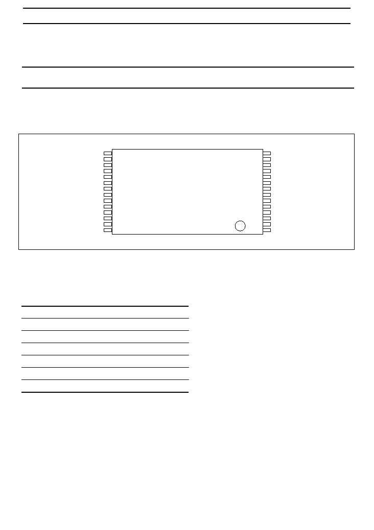
Pin Arrangement
HN58S256AT Series
(Top view)
A2
A1
A0
I/O0
I/O1
I/O2
V
SS
I/O3
I/O4
I/O5
I/O6
I/O7
CE
A10
A3
A4
A5
A6
A7
A12
A14
V
CC
WE
A13
A8
A9
A11
OE
15
16
17
18
19
20
21
22
23
24
25
26
27
28
14
13
12
11
10
9
8
7
6
5
4
3
2
1
Pin Description
Pin name
Function
A0 to A14
Address input
I/O0 to I/O7
Data input/output
OE
Output enable
CE
Chip enable
WE
Write enable
V
CC
Power supply
V
SS
Ground
HN58S256A Series
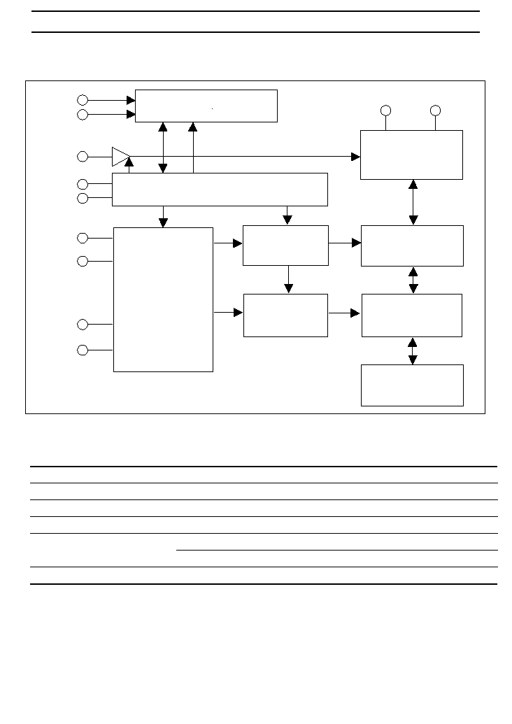
Block Diagram
V
V
OE
CE
A5
A0
A6
A14
WE
CC
SS
I/O0
I/O7
High voltage generator
Control logic and timing
Y decoder
X decoder
Address
buffer and
latch
I/O buffer
and
input latch
Y gating
Memory array
Data latch
to
to
to
Operation Table
Operation
CE
OE
WE
I/O
Read
V
IL
V
IL
V
IH
Dout
Standby
V
IH
◊
*
2
◊
High-Z
Write
V
IL
V
IH
V
IL
Din
Deselect
V
IL
V
IH
V
IH
High-Z
Write inhibit
◊
◊
V
IH
--
◊
V
IL
◊
--
Data
polling
V
IL
V
IL
V
IH
Data out (I/O7)
Notes: 1. Refer to the recommended DC operating condition.
2.
◊
= Don't care

HN58S256A Series
Absolute Maximum Ratings
Parameter
Symbol
Value
Unit
Power supply voltage relative to V
SS
V
CC
≠0.6 to +4.6
V
Input voltage relative to V
SS
Vin
≠0.5*
1
to +4.6*
3
V
Operationg temperature range*
2
Topr
0 to +70
∞
C
Storage temperature range
Tstg
≠55 to +125
∞
C
Notes: 1. Vin min = ≠3.0 V for pulse width
50 ns
2. Including electrical characteristics and data retention
3. Should not exceed V
CC
+ 1.0 V.
Recommended DC Operating Conditions
Parameter
Symbol
Min
Typ
Max
Unit
Supply voltage
V
CC
2.2
3.0
3.6
V
V
SS
0
0
0
V
Input voltage
V
IL
≠0.3*
1
--
0.4
V
V
IH
Vcc
◊
0.7
--
V
CC
+ 0.3*
2
V
Operating temperature
Topr
0
--
70
∞
C
Notes: 1. V
IL
min: ≠1.0 V for pulse width
50 ns.
2. V
IH
max: V
CC
+ 1.0 V for pulse width
50 ns.
DC Characteristics (Ta = 0 to +70
∞
C, V
CC
= 2.2 to 3.6 V)
Parameter
Symbol
Min
Typ
Max
Unit
Test conditions
Input leakage current
I
LI
--
--
2
µ
A
V
CC
= 3.6 V, Vin = 0 to 3.6 V
Output leakage current
I
LO
--
--
2
µ
A
V
CC
= 3.6 V, Vout = 3.6/0.4 V,
CE
= V
IH
, Vin = 0 to 3.6 V
Standby V
CC
current
I
CC1
--
--
10
µ
A
CE
= V
CC
I
CC2
--
--
500
µ
A
CE
= V
IH
Operating V
CC
current
I
CC3
--
--
8
mA
Iout = 0 mA, Duty = 100%,
Cycle = 1
µ
s at V
CC
= 3.6 V
--
--
12
mA
Iout = 0 mA, Duty = 100%,
Cycle = 150 ns at V
CC
= 3.6 V
Output low voltage
V
OL
--
--
0.4
V
I
OL
= 1.0 mA
Output high voltage
V
OH
V
CC
◊
0.8
--
--
V
I
OH
= ≠100
µ
A

HN58S256A Series
Capacitance (Ta = 25
∞
C, f = 1 MHz)
Parameter
Symbol
Min
Typ
Max
Unit
Test conditions
Input capacitance*
1
Cin
--
--
6
pF
Vin = 0 V
Output capacitance*
1
Cout
--
--
12
pF
Vout = 0 V
Note:
1. This parameter is periodically sampled and not 100% tested.
AC Characteristics (Ta = 0 to +70
∞
C, V
CC
= 2.2 to 3.6 V)
Test Conditions
∑
Input pulse levels: 0.4 V to 1.9 V (V
CC
2.7V), 0.4V to 2.4 V (V
CC
> 2.7 V)
∑
Input rise and fall time:
5 ns
∑
Input timing reference levels: 0.8, 1.8 V
∑
Output load: 1TTL Gate +100 pF
∑
Output reference levels: 1.1 V, 1.1 V (V
CC
2.7V),1.5 V, 1.5 V (V
CC
> 2.7 V)
Read Cycle
HN58S256A
-15
-20
Parameter
Symbol
Min
Max
Min
Max
Unit
Test conditions
Address to output delay
t
ACC
--
150
--
200
ns
CE
=
OE
= V
IL
,
WE
= V
IH
CE
to output delay
t
CE
--
150
--
200
ns
OE
= V
IL
,
WE
= V
IH
OE
to output delay
t
OE
10
80
10
100
ns
CE
= V
IL
,
WE
= V
IH
Address to output hold
t
OH
0
--
0
--
ns
CE
=
OE
= V
IL
,
WE
= V
IH
OE
(
CE
) high to output float*
1
t
DF
0
100
0
100
ns
CE
= V
IL
,
WE
= V
IH

HN58S256A Series
Write Cycle
Parameter
Symbol
Min*
2
Typ
Max
Unit
Test conditions
Address setup time
t
AS
0
--
--
ns
Address hold time
t
AH
150
--
--
ns
CE
to write setup time (
WE
controlled)
t
CS
0
--
--
ns
CE
hold time (
WE
controlled)
t
CH
0
--
--
ns
WE
to write setup time (
CE
controlled)
t
WS
0
--
--
ns
WE
hold time (
CE
controlled)
t
WH
0
--
--
ns
OE
to write setup time
t
OES
0
--
--
ns
OE
hold time
t
OEH
0
--
--
ns
Data setup time
t
DS
150
--
--
ns
Data hold time
t
DH
0
--
--
ns
WE
pulse width (
WE
controlled)
t
WP
200
--
--
ns
CE
pulse width (
CE
controlled)
t
CW
200
--
--
ns
Data latch time
t
DL
200
--
--
ns
Byte load cycle
t
BLC
0.4
--
30
µ
s
Byte load window
t
BL
100
--
--
µ
s
Write cycle time
t
WC
--
--
15*
3
ms
Write start time
t
DW
0*
4
--
--
ns
Notes: 1. t
DF
is defined as the time at which the outputs achieve the open circuit conditions and are no
longer driven.
2. Use this device in longer cycle than this value.
3. t
WC
must be longer than this value unless polling techniques is used. This device automatically
completes the internal write operation within this value.
4. Next read or write operation can be initiated after t
DW
if polling techniques is used.
5. A6 through A14 are page addresses and these addresses are latched at the first falling edge
of
WE
.
6. A6 through A14 are page addresses and these addresses are latched at the first falling edge
of
CE
.
7. See AC characteristics.
HN58S256A Series
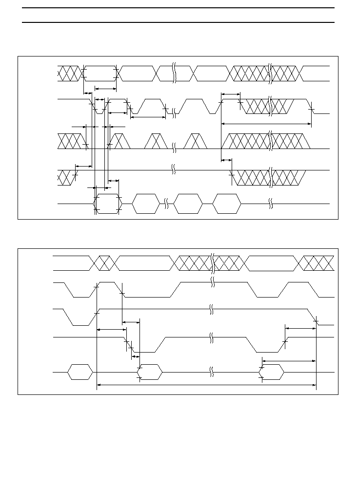
Timing Waveforms
Read Timing Waveform
Address
CE
OE
WE
Data Out
High
Data out valid
t
ACC
t
CE
t
OE
t
OH
t
DF
Byte Write Timing Waveform (1) (
WE Controlled)
Address
CE
WE
OE
Din
t
WC
t
CH
t
AH
t
CS
t
AS
t
WP
t
OEH
t
BL
t
OES
t
DS
t
DH
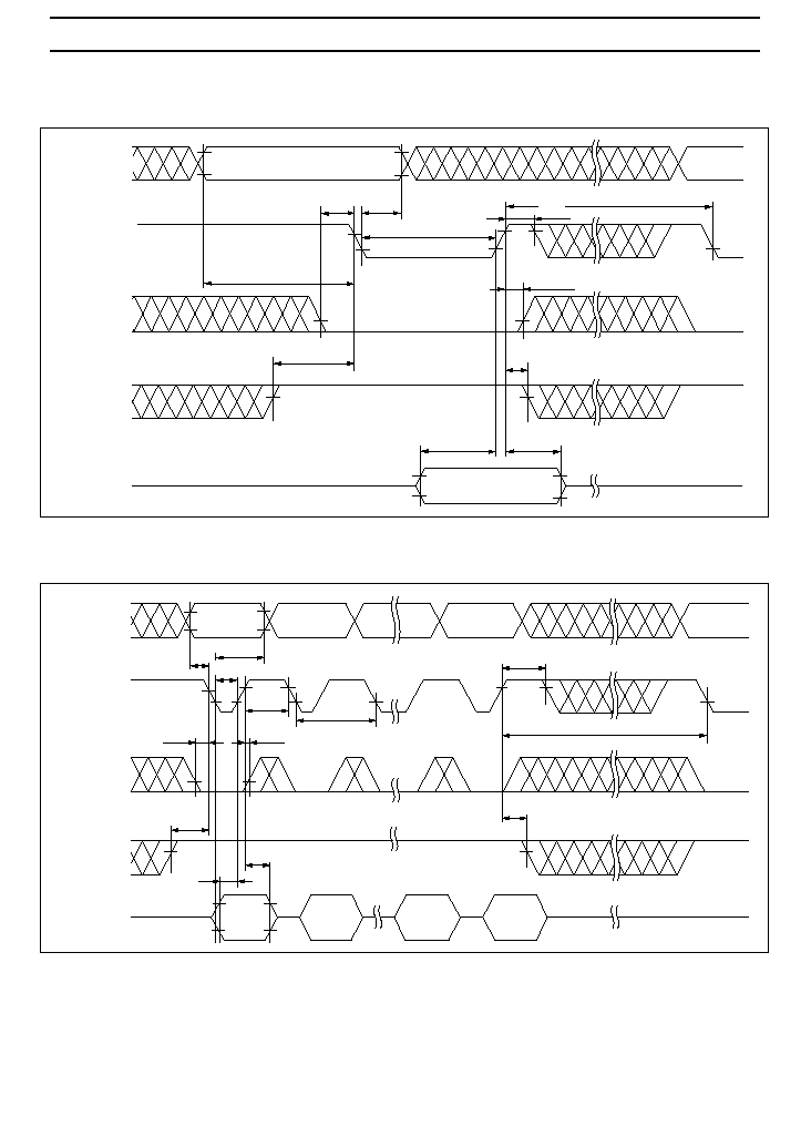
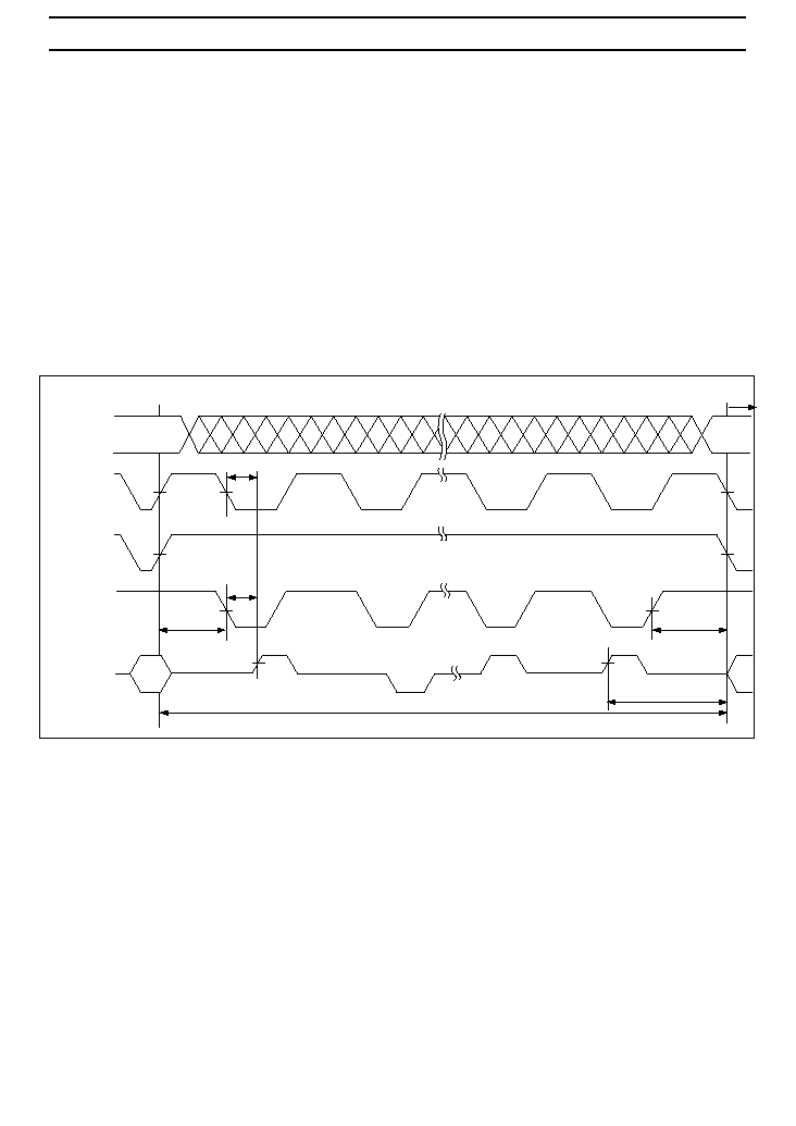
HN58S256A Series
Byte Write Timing Waveform (2) (
CE Controlled)
Address
CE
WE
OE
Din
t
WC
t
AH
t
WS
t
AS
t
OEH
t
WH
t
OES
t
DS
t
DH
t
CW
t
BL
Page Write Timing Waveform (1) (
WE Controlled)
Address
A0 to A14
WE
CE
OE
Din
t
AS
t
AH
t
BL
t
WC
t
OEH
t
DH
t
OES
t
CH
t
CS
t
WP
t
DL
t
BLC
t
DS
*5
HN58S256A Series
Page Write Timing Waveform (2) (
CE Controlled)
Address
A0 to A14
WE
CE
OE
Din
t
AS
t
AH
t
BL
t
WC
t
OEH
t
DH
t
OES
t
WH
t
WS
t
CW
t
DL
t
BLC
t
DS
*5
Data Polling Timing Waveform
t
CE
t
OEH
t
WC
t
DW
t
OES
Address
CE
WE
OE
I/O7
t
OE
Din X
An
An
Dout
X
Dout X
*7
*7
An
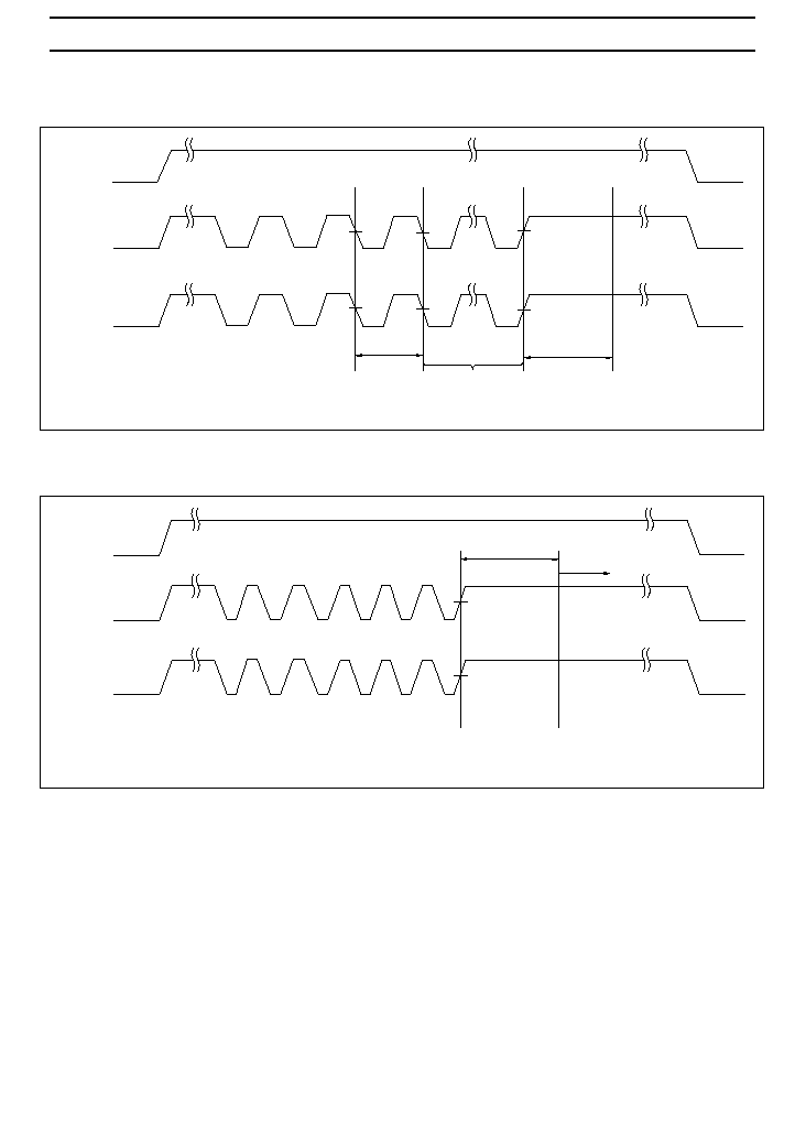
HN58S256A Series
Toggle bit
This device provide another function to determine the internal programming cycle. If the EEPROM is set
to read mode during the internal programming cycle, I/O6 will charge from "1" to "0" (toggling) for each
read. When the internal programming cycle is finished, toggling of I/O6 will stop and the device can be
accessible for next read or program.
Toggle bit Waveform
Notes: 1. I/O6 beginning state is "1".
2. I/O6 ending state will vary.
3. See AS read characteristics.
4. Any address location can be used, but the address must be fixed.
WE
t
OES
OE
CE
Dout
I/O6
Dout
Dout
Dout
Next mode
t
OE
t
CE
t
DW
t
WC
t
OEH
*1
*2
*2
Address
*3
*3
*4
Din
HN58S256A Series
Software Data Protection Timing Waveform (1) (in protection mode)
V
CE
WE
Address
Data
5555
AA
2AAA
55
5555
A0
t
BLC
t
WC
CC
Write address
Write data
Software Data Protection Timing Waveform (2) (in non-protection mode)
V
CE
WE
Address
Data
t
WC
CC
Normal active
mode
5555
AA
2AAA
55
5555
80
5555
AA
2AAA
55
5555
20

HN58S256A Series
Functional Description
Automatic Page Write
Page-mode write feature allows 1 to 64 bytes of data to be written into the EEPROM in a single write
cycle. Following the initial byte cycle, an additional 1 to 63 bytes can be written in the same manner.
Each additional byte load cycle must be started within 30
µ
s from the preceding falling edge of
WE or
CE. When CE or WE is high for 100
µ
s after data input, the EEPROM enters write mode automatically
and the input data are written into the EEPROM.
Data Polling
Data polling allows the status of the EEPROM to be determined. If EEPROM is set to read mode during
a write cycle, an inversion of the last byte of data to be loaded outputs from I/O7 to indicate that the
EEPROM is performing a write operation.
WE, CE Pin Operation
During a write cycle, addresses are latched by the falling edge of
WE or CE, and data is latched by the
rising edge of
WE or CE.
Write/Erase Endurance and Data Retention Time
The endurance is 10
5
cycles in case of the page programming and 10
4
cycles in case of the byte
programming (1% cumulative failure rate). The data retention time is more than 10 years when a device is
page-programmed less than 10
4
cycles.
HN58S256A Series
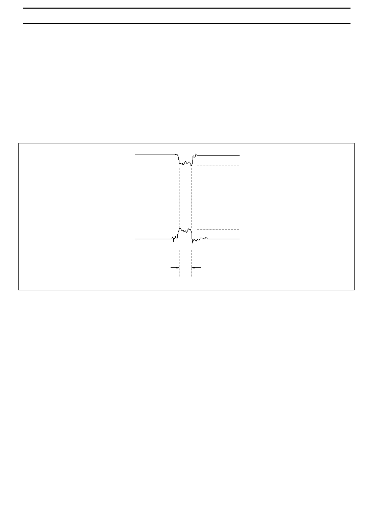
Data Protection
1. Data Protection against Noise on Control Pins (
CE, OE, WE) during Operation
During readout or standby, noise on the control pins may act as a trigger and turn the EEPROM to
programming mode by mistake.
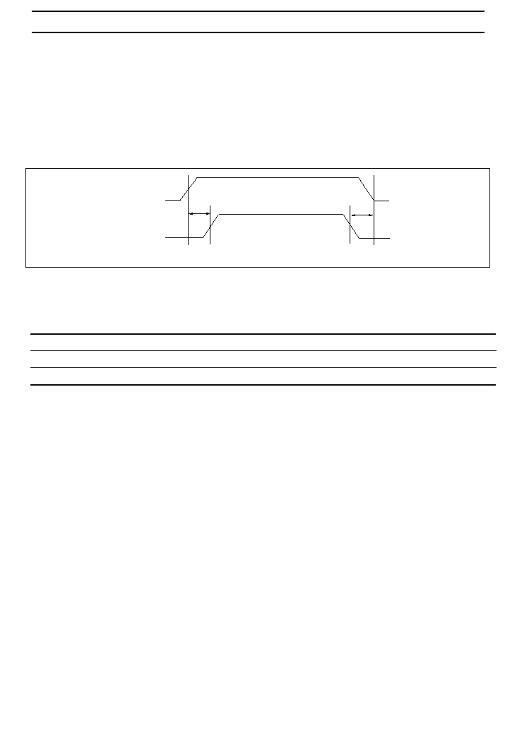
To prevent this phenomenon, this device has a noise cancelation function that cuts noise if its width is 20
ns or less in program mode.
Be careful not to allow noise of a width of more than 20 ns on the control pins.
WE
CE
OE
V
0 V
V
0 V
20 ns max
IH
IH
HN58S256A Series
2. Data Protection at V
CC
On/Off
When V
CC
is turned on or off, noise on the control pins generated by external circuits (CPU, etc) may act
as a trigger and turn the EEPROM to program mode by mistake. To prevent this unintentional
programming, the EEPROM must be kept in an unprogrammable state while the CPU is in an unstable
state.
Note:
The EEPROM shoud be kept in unprogrammable state during V
CC
on/off by using CPU RESET
signal.
V
CC
CPU
RESET
Unprogrammable
Unprogrammable
*
*
(1) Protection by
CE, OE, WE
To realize the unprogrammable state, the input level of control pins must be held as shown in the table
below.
CE
V
CC
◊
◊
OE
◊
V
SS
◊
WE
◊
◊
V
CC
◊
: Don't care.
V
CC
: Pull-up to V
CC
level.
V
SS
: Pull-down to V
SS
level.

HN58S256A Series
3. Software data protetion
To prevent unintentional programming caused by noise generated by external circuits. This device has
the software data protection function. In software data protection mode, 3 bytes of data must be input
before write data as follows. And these bytes can switch the non-protection mode to the protection mode.
SDP is not enabled if only the 3 bytes code is input.
Data
AA
55
A0
Write data }
Address
5555
2AAA
5555
Write address
Normal data input
Software data protection mode can be cancelled by inputting the following 6 bytes. After that, this device
turns to the non-protection mode and can write data normally. But when the data is input in the
cancelling cycle, the data cannot be written.
Data
AA
55
80
AA
55
20
Address
5555
2AAA
5555
5555
2AAA
5555
The software data protection is not enabled at the shipment.
Note:
There are some differences between Hitachi's and other company's for enable/disable sequence
of software data protection. If there are any questions , please contact with Hitachi sales offices.
HN58S256A Series
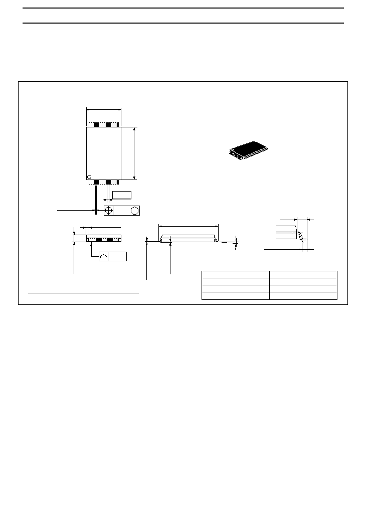
Package Dimensions
HN58S256AT Series (TFP-28DB)
0.10
M
0.55
8.00
0.22
±
0.08
13.40
±
0.30
0.17
±
0.05
0.13
1.20 Max
11.80
0
∞
≠ 5
∞
28
1
14
15
8.20 Max
0.10
+0.07 ≠0.08
0.50
±
0.10
0.80
0.45 Max
Hitachi Code
JEDEC Code
EIAJ Code
Weight (reference value)
TFP-28DB
--
--
0.23 g
0.20
±
0.06
0.15
±
0.04
Unit: mm
Dimension including the plating thickness
Base material dimension

HN58S256A Series
When using this document, keep the following in mind:
1. This document may, wholly or partially, be subject to change without notice.
2. All rights are reserved: No one is permitted to reproduce or duplicate, in any form, the whole or part
of this document without Hitachi's permission.
3. Hitachi will not be held responsible for any damage to the user that may result from accidents or any
other reasons during operation of the user's unit according to this document.
4. Circuitry and other examples described herein are meant merely to indicate the characteristics and
performance of Hitachi's semiconductor products. Hitachi assumes no responsibility for any
intellectual property claims or other problems that may result from applications based on the examples
described herein.
5. No license is granted by implication or otherwise under any patents or other rights of any third party
or Hitachi, Ltd.
6. MEDICAL APPLICATIONS: Hitachi's products are not authorized for use in MEDICAL
APPLICATIONS without the written consent of the appropriate officer of Hitachi's sales company.
Such use includes, but is not limited to, use in life support systems. Buyers of Hitachi's products are
requested to notify the relevant Hitachi sales offices when planning to use the products in MEDICAL
APPLICATIONS.
Hitachi, Ltd.
Semiconductor & IC Div.
Nippon Bldg., 2-6-2, Ohte-machi, Chiyoda-ku, Tokyo 100, Japan
Tel: Tokyo (03) 3270-2111
Fax: (03) 3270-5109
For further information write to:
Hitachi America, Ltd.
Semiconductor & IC Div.
2000 Sierra Point Parkway
Brisbane, CA. 94005-1835
U S A
Tel: 415-589-8300
Fax: 415-583-4207
Hitachi Europe GmbH
Electronic Components Group
Continental Europe
Dornacher Straþe 3
D-85622 Feldkirchen
M¸nchen
Tel: 089-9 91 80-0
Fax: 089-9 29 30 00
Hitachi Europe Ltd.
Electronic Components Div.
Northern Europe Headquarters
Whitebrook Park
Lower Cookham Road
Maidenhead
Berkshire SL6 8YA
United Kingdom
Tel: 0628-585000
Fax: 0628-778322
Hitachi Asia Pte. Ltd.
16 Collyer Quay #20-00
Hitachi Tower
Singapore 0104
Tel: 535-2100
Fax: 535-1533
Hitachi Asia (Hong Kong) Ltd.
Unit 706, North Tower,
World Finance Centre,
Harbour City, Canton Road
Tsim Sha Tsui, Kowloon
Hong Kong
Tel: 27359218
Fax: 27306071