Äîêóìåíòàöèÿ è îïèñàíèÿ www.docs.chipfind.ru

CONTENTS
Accepted by :
3284PS 2701 - SX21V001-Z4A - 3
June 10,'99
SX21V001-Z4A
3284PS 2701 - SX21V001-Z4A - 3
3284PS 2702 - SX21V001-Z4A - 3
3284PS 2703 - SX21V001-Z4A - 3
3284PS 2704 - SX21V001-Z4A - 3
3284PS 2705 - SX21V001-Z4A - 3
3284PS 2706 - SX21V001-Z4A - 3
3284PS 2707 - SX21V001-Z4A - 3
3284PS 2708 - SX21V001-Z4A - 3
3283PS 2709 - SX21V001-Z4A - 3
3284PS 2710 - SX21V001-Z4A - 3
3284PS 2711 - SX21V001-Z4A - 3
3284PS 2712 - SX21V001-Z4A - 3
3284PS 2713 - SX21V001-Z4A - 3
1-1/1
2-1/1
3-1/1
4-1/1
5-1/2
5-2/2
6-1/3
6-3/3
7-1/1
8-1/7
8-7/7
9-1/2
9-2/2
10-1/4
10-4/4
11-1/3
11-3/3
12-1/2
12-2/2
13-1/1
Page
1-1/1
Proposed by :
Displays, Hitachi, Ltd.
Sh.
No.
Displays, Hitachi, Ltd.
3300 Hayano, Mobara City
Chiba Pref. 297 Japan
TEL : +81-475-25-9005 (Dial In)
FAX : +81-475-22-5217
For Messrs :
Date :
CUSTOMER'S ACCEPTANCE SPECIFICATIONS
1
2
3
4
5
6
7
8
9
10
11
12
13
COVER
RECORD OF REVISION
MECHANICAL DATA
ABSOLUTE MAXIMUM RATINGS
ELECTRICAL CHARACTERISTICS
OPTICAL CHARACTERISTICS
BLOCK DIAGRAM
INTERFACE TIMING CHART
DIMENSIONAL OUTLINE
APPEARANCE STANDARD
PRECAUTION IN DESIGN
DESIGNATION OF LOT MARK
PRECAUTION FOR USE
No.
ITEM
Sheet No.
Page

Displays,
Hitachi, Ltd.
Sh.
No.
Page
Date
3284PS 2702 - SX21V001-Z4A - 3
June 10, '99
2-1/1
RECORD OF REVISION
Date
May 25,'99
3284PS 2712-
SX21V001-Z4A-2
Page 12-2/2
Sheet No.
Summary
12.2 REVISION
Added Rev.B
June 10,'99
5.2.2 ELECTRICAL CHARACTERISTICS
Revised resistance betw een terminal
X1-X2 : 350
850
400
800
Y1-Y2 : 350
750
220
700
3284PS 2705-
SX21V001-Z4A-3
Page 5-2/3

3284PS 2703 - SX21V001-Z4A - 3
June 10, '99
3-1/1
3. MECHANICAL DATA
(1) Part Name
(2) Module Size
(3) Display Size
(4) Dot Pitch
(5) Number of Dots
(6) Duty
(7) LCD
(8) View ing Direction
(9) Backlight
(10) Weight
(11) Pow er Supply Voltage
(12) Touch panel
SX21V001-Z4A
203.0(W) mm
×
142.5(H) mm
×
8.0 max (D) mm
167.02(W) mm
×
125.26(H) mm
Diagonal size 21cm (8.2")
0.087(W) mm
×
0.261(H) mm
640
×
3 (R,G,B)(W)
×
480 (H) dots
1/240
Film type (negative type)
12 O'clock
Cold Cathode Fluorescent Lamp (CFL)
×
1
(310) g typ
3.3V only
Resistance type
Displays,
Hitachi, Ltd.
Sh.
No.
Page
Date

3284PS 2704 - SX21V001-Z4A - 3
June 10, '99
4-1/1
4. ABSOLUTE MAXIMUM RATINGS
Displays,
Hitachi, Ltd.
Sh.
No.
Page
Date
4. 1 ELECTRICAL ABSOLUTE MAXIMUM RATINGS (LCM)
ITEM
Note 1 DISP OFF, FLM, CL1, CL2, UD0
UD7, LD0
LD7
Note 2 Make certains you are grounded w hen handling LCM
4. 3 ENVIRONMENTAL ABSOLUTE MAXIMUM RATINGS
ITEM
Note 1 Ta<40
°
C : 85%RH max.
Ta>40
°
C : Absolute humidity must be low er than the humidity of 85%RH at 40
°
C.
Note 2 Ta at -20
°
C ---------- <48h, at 60
°
C ---------- <168h
Note 3 Background color changes slightly depending on ambient temperature.
This phenomenon is reversible.
Note 4 5Hz
100Hz (Except resonance frequency)
Note 5 This module should be operated normally af ter finish the test.
Note 6 When LCM is operated at 5°C, the life time of CFL w ill be reduced.
Need to make sure of value of IL and characteristics of inverter.
Also the response time at 5°C w ill be slow er.
Ambient Temperature
Humidity
Vibration
Shock
Corrosive Gas
OPERATING
MIN
5
°
C
Note 1
-
-
Not Acceptable
MAX
40
°
C
2.45 m/s
2
(0.25G)
29.4 m/s
2
(3G)
STORAGE
MIN
-20
°
C
Note 1
-
-
Not Acceptable
MAX
60
°
C
11.76 m/s
2
(1.2G)
490 m/s
2
(50G)
Note 5
Note 5
COMMENT
Note 2, 3
Without condensation
Note 4
XYZ directions 11ms
VSS=0V:Standard
Pow er Supply for Logic
Contrast Adjustment Voltage
Input Voltage
Input Current
Static Electricity
SYMBOL
VDD-VSS
VCON-VSS
Vi
Ii
-
MIN
0
0
-0.3
0
-
MAX
6.0
VDD
VDD+0.3
1
-
UNIT
V
V
V
A
-
COMMENT
Note 1
Note 2
4. 2 ELECTRICAL ABSOLUTE MAXIMUM RATINGS (TOUCH PANEL)
ITEM
Voltage
Current
SPECIFICATION
(7VDC) (MAX)
(25mA) (max)
NOTE

Displays,
Hitachi, Ltd.
Sh.
No.
Page
Date
3284PS 2705 - SX21V001-Z4A - 3
June 10, '99
5-1/3
5. ELECTRICAL CHARACTERISTICS
5. 1 ELECTRICAL CHARACTERISTICS OF LCD
ITEM
VSS=0V
Pow er Supply Voltage
VDD
VCON
Vi
IDD
Icon(Note5)
Iin (Note2)
Vcon
fFLM
Contrast Adjustment
VDD-VSS=3.3V
-
"H" level
"L" level
VDD-VSS=3.3V
Vcon=0.8
2.8V
Vin=VDDorVSS
Ta= 5
°
C,
=
0
°
Ta=25
°
C,
=
0
°
Ta=40
°
C,
=
0
°
-
Voltage
(Note 1)
Input Voltage for Logic
Circuits
(Note 2)
Pow er Supply Current
(Note 3)
Input Leak Current
Contrast Adjustment
Voltage
(Note 6)
Frame Frequency
(Note 7)
SYMBOL
CONDITION
MIN
TYP
MAX
UNIT
3.15
0.8
0.8VDD
0
-
-
-
0.8
-
-
100
3.30
-
-
-
30
-
-
-
(1.8)
-
120
3.45
2.8
VDD
0.2VDD
46
(20)
±
1.0
-
-
2.8
150
V
V
V
mA
V
Hz
µ
A
(Note 1) In proportion as the VCON voltage decrease the brightness w ill increase.
(Note 2) DISP OFF, FLM, CL1, CL2, UD0
UD7, LD0
LD7
(Note 3) f FLM=120Hz, Ta=25
°
C, Display pattern:Checker pattern.
(Note 4) Rush Current of Pow er ON : 2A(PK)
×
100
µ
s
(Note 5) VCON
(Note 6) The Contrast Adjustment Voltage fluctuates about
±
0.3V by each module.
(only TYP values)
(Note 7) Need to make sure of flickering and rippling of display w hen setting the Frame Frequency
in your set.
(Note 8) Absolute maximum ratings voltage of CFL cable for this module is as follow s.
VCFL side : 2kV
VSS side : 300V
This inverter design shall not exceed the rated voltage.

Displays,
Hitachi, Ltd.
Sh.
No.
Page
Date
3284PS 2705 - SX21V001-Z4A - 3
June 10, '99
5-2/3
5. 2 ELECTRICAL CHARACTERISTICS OF TOUCH PANEL
ITEM
Operating Voltage
Operating Current
SPECIFICATION
5VDC
10
25mA
5.2.1 OPERATING CONDITION
ITEM
Resistance
betw een terminal
Insulance Resistance
SPECIFICATION
220
700
5.2.2 ELECTRICAL CHARACTERISTICS
Linearity
Chattering
X1-X2
Y1-Y2
X-Y
X
Y
400
800
10M
min
1.5% max
1.5% max
10msec max
Operating Voltage
See Note 1
NOTE
ITEM
Pen input pressure
Surface hardness
SPECIFICATION
2H min
5.2.3 MECHANICAL CHARACTERISTICS
0.05N
0.5N
NOTE
JIS K 5400
ITEM
Transparency
SPECIFICATION
5.2.4 OPTICAL CHARACTERISTICS
81% typ
NOTE

Displays,
Hitachi, Ltd.
Sh.
No.
Page
Date
3284PS 2705 - SX21V001-Z4A - 3
June 10, '99
5-3/3
5. 3 ELECTRICAL CHARACTERISTICS OF BACKLIGHT
ITEM
(Note 1) Please design your lamp driving circuit (inverter) according to the above specifications,
and inf orm Hitachi of it.
(Note 2) Starting discharge voltage is increased w hen LCM is operating at low er temperature.
Please check the characteristics of your inverter before applying to your set.
(Note 3) Average life time of CFL w ill be decreased w hen LCM is operating at low er temperature.
(Note 4) Under low er driving frequency of an inverter, a certain backlight system (CFL & CFL
reflection sheet) may generate a sound noise. Before designing the inverter, please
consider the driving frequency and the noise.
(Note 5) Under low er temperature, please check CFL characteristics on your inverter.
(Note 6)
Lamp Voltage
Frequency
Lamp Current (1Lamp) (Note6)
Starting discharge Voltage
SYMBOL
VL
fL
IL
VS
(Note 2)
MIN
-
-
(1.2)
(Note 2)
(1400)
TYP
(500)
(60)
-
(1.8)
MAX
-
-
(2.5)
(Note 2)
-
UNIT
Vrms
kHz
Vrms
mA
NOTE
Ta=25°C
Ta=25°C
Ta=5°C
GND
INV
H.V
A
Note 1 : Test Methode and Conditions
The difference ("e") betw een the theoretical output voltage and the actual output voltage w hen
pressure is applied to any point w ithin the valid area must be as indicated below .
e < applied voltage
×
0.03 (=
±
0.015)
Ag electrode
Resistor
Ag electrode
XL
X
Valid area
E
rB
rA
rA, rB = Resistance of Pattern
Ea
Eb
e
XL min
XL max
Valid area
E(v)
Dashed line :
Theoretically
correct voltage
Solid line :
Output voltage
(same Y line)

3284PS 2706 - SX21V001-Z4A - 3
June 10, '99
6-1/3
6.1 OPTICAL CHARACTERISTICS OF LCD
6. OPTICAL CHARACTERISTICS
ITEM
Ta=25
°
C (Backlight On)
(Measurement condition : Hitachi standard)
Note 1)
7) : See next page.
View ing area
Contrast ratio
Response time (rise)
Response time (f all)
Color tone
(Primary Color)
SYMBOL
2-
1
K
tr
tf
x
y
Red
x
y
x
y
x
y
Green
Blue
White
CONDITION
=0
°
, K>2.0
=0
°
,
=0
°
=0
°
,
=0
°
=0
°
,
=0
°
=0
°
,
=0
°
MIN
-
-
-
-
-
-
-
-
-
-
-
-
TYP
(40)
(50)
(190)
(160)
(0.54)
(0.33)
(0.31)
(0.51)
(0.17)
(0.17)
(0.29)
(0.31)
MAX
-
-
-
-
-
-
-
-
-
-
-
-
UNIT
deg
-
ms
ms
-
-
-
-
-
-
-
-
NOTE
1),2)
3),5),6)
4)
4)
7)
Displays,
Hitachi, Ltd.
Sh.
No.
Page
Date

3284PS 2706 - SX21V001-Z4A - 3
June 10, '99
6-2/3
Note 1. Definition of
and
(Normal)
View ing direction
Note 3. Definition of contrast "K"
Note 2. Definition of view ing angle
1 and
2
X
y (
=180
°
)
y' (
=0
°
)
X'
Z
1
2
K =
Brightness on non-selected area (B2)
Brightness on selected area (B1)
B1
B2
Operation voltage
(B1)
(Di="H")
(B2)
(Di="L")
K
2.0
1
2
1<0
°
<
2
Contrast ratio K vs view ing angle
=0
°
Sensor
Back light
Sensor : BM-7 or correspondence
equipment
Note 4. Definition of optical response time
Note 5. Hitachi w ill not do 100% inspection for minimum value. Minimum value is for reference.
Note 6. Hitachi w ill do sampling inspection for minimum value.
Note. 7 The LCD driving voltage should be adjusted at the voltage w here the peak contrast is obtained.
Non-selective state
selective state
Non-selective state
100%
90%
10%
tr
Rise time
tf
Fall time
Displays,
Hitachi, Ltd.
Sh.
No.
Page
Date

3284PS 2706 - SX21V001-Z4A -3
June 10, '99
6-3/3
6.2 OPTICAL CHARACTERISTICS OF BACKLIGHT
ITEM
NOTE
TYP
MAX
UNIT
MIN
Brightness
Rise Time
Brightness Unif ormity
-
-
-
(58)
5
-
-
-
±
30
cd/m
2
Minute
%
IL=1.8mA
Note 1),2)
IL=1.8mA
Brightness 80%
Undermentioned
Note 1),4)
Measurement condition : Hitachi standard)
CFL : INITIAL, Ta=25
°
C
Display data should be all "ON"
The LCD driving voltage should be adjusted at the voltage w here the peak contrast is obtained,
w hen set pattern is all "Q".
(Note 1) Measurement af ter 10 minutes from CFL operating.
Average value of 9 points (Note 3).
(Note 2) Brightness control : 100%
(Note 3) Measurement of the follow ing 9 places on the display.
X=70
X=240
X=410
P1
P4
P7
P2
P5
P8
P3
P6
P9
Y=180 Y=960 Y=1740
(Note 4) Definition of the brightness tolerance.
Max brightness or Min brightness - Average brightness
Average brightness
×
100
Displays,
Hitachi, Ltd.
Sh.
No.
Page
Date

3284PS 2707 - SX21V001-Z4A - 3
June 10, '99
7-1/1
7. BLOCK DIAGRAM
CN2
VCFL
VSS
CFL
Buffer
Buffer
Pow er
Supply
Circuit
LCD PANEL
Column driv ing circuit (Upper)
Column driv ing circuit (Lower)
X1
X480
Timing
Circuit
Buffer
Timing
Circuit
M
DISP
·
OFF
CN1
FLM
CL1
CL2
DISP
·
OFF
UD7~
UD0
LD7~
LD0
VDD
VSS
VCON
Displays,
Hitachi, Ltd.
Sh.
No.
Page
Date

3284PS 2708 - SX21V001-Z4A - 2
May 25, '99
8-1/7
8. INTERFACE TIMING CHART
8.1 TIMING CHART
Note(1) : The interval of CL1 pulse must be same including the vertical blanking period.
Displays,
Hitachi, Ltd.
Sh.
No.
Page
Date
FLM
CL1
CL2
UD7
UD6
UD0
CL1
FLM
LD0~LD7
R
B
G
Y1
Y9
Y1913
G
R
B
Y2
Y10
Y1914
R
B
G
Y7
Y15
Y1919
G
R
B
Y8 Y16
Y1920
UD1
UL7
LD6
LD0
R
B
G
Y1921 Y1929
Y1913
G
R
B
Y1922 Y1930
Y1914
R
B
G
Y1927 Y1935
Y1919
G
R
B
Y1928 Y1936
Y1920
LD1
X1
X2
Y240
Dummy data
X241 X242
Y480
Dummy data
Y239
Y479
(Reduction)
(240+n)
×
T
X241
X242
Dummy data
X1
X2
Dummy data
Note(1)
UD0~UD7

3284PS 2708 - SX21V001-Z4A - 2
May 25, '99
8-2/7
8.2 INTERFACE TIMING SPECIFICATION
ITEM
SYMBOL
MIN
TYP
MAX
UNIT
ns
ns
ns
ns
ns
ns
ns
ns
ns
ns
30
65
50
100
40
15
20
10
50
10
tWHCL1
tCYC
tWCL2
tSCL1
tHCL1
tr, tf
tDSU
tDH
tFS
tFH
CL1 pulse w idth "H"
Clock cycle time
CL2 pulse w idth
Clock set up time
Clock hold time
Clock rise fall time
Data set up time
Data hold time
"FLM" set up time
"FLM" hold time
VDD=3.3
±
0.15V, VSS=0V, Vcon=0.8~2.8V, Ta=+5
°
C~+40
°
C
0.9VDD
0.8VDD
0.2VDD
0.8VDD
0.2VDD
MEASUREMENT POINT
0.9VDD
0.1VDD
UDO~UD7
LDO~LD7
CL2
CL1
FLM
tFH
tFS
tWHCL1
tr
tf
tWHCL2
tr
tf
tSCL1
tHCL1
tWCL2
tCYC
tDH
tDSU
0.1VDD
Displays,
Hitachi, Ltd.
Sh.
No.
Page
Date

3284PS 2708 - SX21V001-Z4A - 2
May 25, '99
8-3/7
8.3 POWER ON / OFF SEQUENCE
SYMBOL
MIN
MAX
UNIT
ms
ms
ms
ns
ns
ms
ms
ms
ms
100
200
200
0
20
0
0
20
tDLD
tCH
tLDH
tDOr
tDOf
tDLCr
tDLCf
tDLCs
tVH
COMMENT
(Note 1)
(Note 2)
100
(Note 1) Please keep the specif ied sequence because w rong sequence may
cause permanent damage to the LCD panel.
(Note 2) Hitachi recommends you to use DISP
·
OFF function.
Display quality may deteriorate if you don't use DISP
·
OFF function.
VDD
tDLD
tDLD
tCH
tCH
tDLCr
tDLCf
tDLCs
tDLCs
tLDH
tLDH
tDOr
tDOf
tVH
CL1
VCON
DISP
·
OFF
3.15V
3.15V
0.8
×
VDD
0.8
×
VDD
0.8
×
VDD
0.2
×
VDD
Displays,
Hitachi, Ltd.
Sh.
No.
Page
Date

3284PS 2708 - SX21V001-Z4A - 3
June 10, '99
8-4/7
8.4 POWER SUPPLY FOR LCM
Displays,
Hitachi, Ltd.
Sh.
No.
Page
Date
VCFL
VSS
CFL
VCON
VDD
VSS
C2
+
-
+3.3V
C1
+
-
Stabilized
+3.3V
R1
R2
VR
LCM

3284PS 2708 - SX21V001-Z4A - 3
June 10, '99
8-5/7
8.5 INPUT DATA ALLOCATION TABLE
Displays,
Hitachi, Ltd.
Sh.
No.
Page
Date
U U U U U U U U U U U U U U U U U
D D D D D D D D D D D D ----- D D D D D
7 6 5 4 3 2 1 0 7 6 5 4 4 3 2 1 0
Data Signal
Y
X
1
2
3
4
5
238
239
240
241
242
243
244
245
478
479
480
Data Signal
X
Y
1 2 3 4 5 6 7 8 9 10 11 12 1 1 1 1 1
----- 9 9 9 9 9
1 1 1 1 2
6 7 8 9 0
1 1 1 1 1 1 1 1 1 1 1 1 3 3 3 3 3
9 9 9 9 9 9 9 9 9 9 9 9 ----- 8 8 8 8 8
2 2 2 2 2 2 2 2 2 3 3 3 3 3 3 3 4
1 2 3 4 5 6 7 8 9 0 1 2 6 7 8 9 0
R G B R G B R G B R G B ----- G B R G B
R G B R G B R G B R G B ----- G B R G B
R G B R G B R G B R G B ----- G B R G B
R G B R G B R G B R G B ----- G B R G B
R G B R G B R G B R G B ----- G B R G B
R G B R G B R G B R G B ----- G B R G B
R G B R G B R G B R G B ----- G B R G B
R G B R G B R G B R G B ----- G B R G B
R G B R G B R G B R G B ----- G B R G B
R G B R G B R G B R G B ----- G B R G B
R G B R G B R G B R G B ----- G B R G B
R G B R G B R G B R G B ----- G B R G B
R G B R G B R G B R G B ----- G B R G B
R G B R G B R G B R G B ----- G B R G B
R G B R G B R G B R G B ----- G B R G B
R G B R G B R G B R G B ----- G B R G B
L L L L L L L L L L L L L L L L L
D D D D D D D D D D D D ----- D D D D D
7 6 5 4 3 2 1 0 7 6 5 4 4 3 2 1 0

3284PS 2708 - SX21V001-Z4A - 3
June 10, '99
8-6/7
8.6 INTERNAL PIN CONNECTION
CN1 MOLEX 54104-3511
PIN No.
SIGNAL
LEVEL
FUNCTION
1
2
3
4
5
6
7
8
9
10
11
12
13
14
15
16
17
18
19
20
21
22
23
24
25
26
27
28
29
30
31
32
33
34
35
LD0
LD1
LD2
LD3
VSS
LD4
LD5
LD6
LD7
VSS
FLM
CL1
VSS
CL2
VSS
VDD
VDD
VCON
VSS
VDD
UD0
UD1
UD2
UD3
VSS
UD4
UD5
UD6
UD7
VSS
DIG Y2
DIG X2
DIG Y1
DIG X1
H / L
Display Data (Low er Column)
First Line Marker
H : ON / L : OFF
Data Latch
GND
Data Shif t
GND
Pow er Supply for Logic
Pow er Supply for Logic
Contrast Adjust
GND
GND
Display Data (Upper Column)
H / L
H / L
H / L
-
H / L
H / L
H / L
H / L
-
H
H / L
H / L
H / L
H / L
H / L
H / L
H / L
H / L
H / L
-
-
-
-
-
-
-
-
-
-
-
-
-
H L
H L
Display Data (Low er Column)
Display Data (Low er Column)
Display Data (Low er Column)
GND
Display Data (Low er Column)
Display Data (Low er Column)
Display Data (Low er Column)
Display Data (Low er Column)
GND
Display Data (Upper Column)
Display Data (Upper Column)
Display Data (Upper Column)
GND
Display Data (Upper Column)
Display Data (Upper Column)
Display Data (Upper Column)
Display Data (Upper Column)
GND
Touch panel Y2
Touch panel X2
Touch panel Y1
Touch panel X1
DISP
·
OFF
Displays,
Hitachi, Ltd.
Sh.
No.
Page
Date

3284PS 2708 - SX21V001-Z4A - 3
June 10, '99
8-7/7
Displays,
Hitachi, Ltd.
Sh.
No.
Page
Date
GND for CFL
Pow er Supply for CFL
-
A C
VSS
VCFL
FUNCTION
LEVEL
SIGNAL
2
1
PIN No.
CN2 JST : BHSR-02VS-1 (Suitable Connector : (1) SM02B-BHSS-1-TB or
or
(1) housing : BHSMR-02VS-1
contact pin : SBHSM-002T-P0.5


3284PS 2710 - SX21V001-Z4A - 3
June 10, '99
10-1/4
10.1 APPEARANCE INSPECTION CONDITION
Visual inspection should be done under the follow ing condition.
(1) The inspection should be done in a dark room.
(2) The CFL should be lighted w ith the prescribed inverter.
(3) The distance betw een eyes of an inspector and the LCD Module is 25cm.
(4) The view ing zone is show n the f igure.
View ing angle < 25
°
10. APPEARANCE STANDARD
10.2 DEFINITION OF ZONE
A zone : The effective display area specif ied at page 9-1/2 of this document.
B zone : Area betw een the w indow of bezel line and the eff ective display are (A zone) line
specified at page 9-1/2 of this document.
25
°
eye
25
°
eye
LCD
Bezel
Dots area
Effective display area
A zone
B zone
Displays,
Hitachi, Ltd.
Sh.
No.
Page
Date

10.3 APPEARANCE SPECIFICATION
(1) LCD APPEARANCE
*) If the problem related to this section occurs about this item, the responsible persons of both
party (Customer and HITACHI) w ill discuss the matter in detail.
ITEM
Distinguished one is not acceptable
(To be judged by HITACHI STANDARD)
Same as above
Same as above
Average diameter D (mm)
D < 0.2
0.2 < D < 0.3
0.3 < D < 0.5
0.5 < D
Maximum acceptable number
ignored
12
3
none
Filamentous (Line shape)
L < 2.0
L < 3.0
L < 2.5
0.03 < W < 0.05
0.05 < W < 0.1
W < 0.03
Length L (mm)
Width W (mm)
Maximum
acceptable number
ignored
6
1
Round (Dot shape)
Maximum
acceptable number
Average
diameter D (mm)
Minimum space
0.2 < D < 0.3
D < 0.2
0.3 < D < 0.4
0.4 < D
The total number
ignored
10
5
none
10 mm
30 mm
Filamentous + Round = 10
Those w iped out easily are acceptable
CRITERIA
APPLIED
ZONE
To be judged by HITACHI STANDARD
Same as above
A
A
A,B
A,B
A
A
A
A
Scratches
No.
Dent
Wrinkles in Polarizer
Bubbles
Stains,
Foreign
materials
Dark spot
Color tone
Color uniformity
L
C
D
3284PS 2710 - SX21V001-Z4A - 1
May 25, '99
10-2/4
Displays,
Hitachi, Ltd.
Sh.
No.
Page
Date

3284PS 2710 - SX21V001-Z4A - 3
June 10, '99
10-3/4
ITEM
D<0.25
0.25<D<0.35
ignored
none
W < 0.25
W < 0.2
W < 0.15
Maximum
acceptable
CRITERIA
APPLIED
ZONE
A
A
Contrast irregularity
(Spot)
No.
L
C
D
Average
diameter
D (mm)
0.35<D<0.5
0.5<D<0.7
0.7<D
number
Minimum
space
Contrast
3
Maximum
acceptable
number
W < 0.1
Width
W (mm)
4
10
To be
judged by
HITACHI
STANDARD
Length
L (mm)
L < 1.2
L < 1.5
L < 2.0
L < 3.0
2
3
3
4
50mm
20mm
20mm
Minimum
space
20mm
20mm
20mm
20mm
6
The w hole number
Contrast irregularity
(Line)
(A pair of scratches)
To be judged by HITACHI STANDARD
Rubbing Scratch
ITEM
D < 0.4
0.4 < D
ignored
Maximum Acceptable number
CRITERIA
APPLIED
ZONE
A
A
No.
C
F
L
B
A
C
K
L
I
G
H
T
Average diameter D (mm)
Maximum
acceptable number
Width W (mm)
none
Foreign materials
(Line)
Scratches
(2) CFL BACKLIGHT APPEARANCE
Dark spots
White spots
Foreign materials
(Spot)
Length L (mm)
L < 2.5
2.5 < L
1
none
none
W < 0.2
0.2 < W
Maximum
acceptable number
Width W (mm)
Length L (mm)
L < 11.0
11.0 < L
1
none
none
W < 0.1
0.1 < W < 0.2
0.2 < W
ignored
A
Displays,
Hitachi, Ltd.
Sh.
No.
Page
Date

3284PS 2710 - SX21V001-Z4A - 3
June 10, '99
10-4/4
Displays,
Hitachi, Ltd.
Sh.
No.
Page
Date
Note (1) Definition of Average diameter (D)
b
D =
a+b
2
Note (2) Definition of Length (L) and Width (W)
L
ITEM
D < 0.25
0.25 < D < 0.35
ignored
Criteria
CRITERIA
APPLIED
ZONE
A
A
No.
T
O
U
C
H
P
A
N
E
L
Average diameter D (mm)
6
(3) TOUCH PANEL APPEARANCE
Foreign material
(Black or White spots)
A
Foreign material (Line)
or
Scratches
Fisheyes on film surface
Uncleanliness
Crack in glass plate
0.35 < D
none
W < 0.05
0.05 < W < 0.1
ignored
Criteria
Width W (mm)
0.1 < W
10 < L : none
L < 10 : 4
Spote spec
D < 0.2
0.2 < D < 0.35
ignored
Criteria
Average diameter D (mm)
6
0.35 < D < 0.6
none
0.6 < D
2
No conspicuous dirt
No cracks are allow ed
A
A

11. PRECAUTION IN DESIGN
11. 1 MOUNTING PRECAUTION
3284PS 2711 - SX21V001-Z4 A- 3
June 10, '99
11-1/4
Please mount the LCD Module using mounting holes arranged in 4 corners, and please pay attention
to the f ollow ings.
Displays,
Hitachi, Ltd.
Sh.
No.
Page
Date
(1) To prevent the module cover from being pressed, the distance betw een the module and the
f itting plate, w hich means the lenght of the spacers, should be shorter than 1.0mm.
(2) We recommend you to use protective spacers in order to protect the module from any kinds of
shocks to your set.
(3) For the module to be used at upright position, the case shall have a structure w here the touch
panel screen does not shif t w ith its ow n w eight.
The module
Spacer
Spacer
Customer's housing
Protective spacer
Example of mounting
18.0
106.0
198.5
±
0.2
99.0
6.0
Upper panel
Low er panel
Protective spacer
4-
5.0
Spacer 4-
6.0
Location of spacers
Unit : mm
Scale : NTS
Touch panel
3284PS 2711 - SX21V001-Z4A - 3
June 10, '99
11-2/4
Displays,
Hitachi, Ltd.
Sh.
No.
Page
Date
11.3 POWER ON SEQUENCE
Input signals should not be applied to LCD module before pow er supply voltage is applied and
reaches to specified voltage (3.0
±
0.15V).
If the above sequence is not kept, C-MOS LSIs of LCD module may be damaged due to latch up
phenomenon.
11.4 HANDLING PRECAUTIONS
(1) Since the polarizer on the top, and the aluminum plate on the bottom tend to be easily damaged,
they should be handled w ith full care so as not to get them touched, pushed or rubbed by a piece
on glass, tw eezers and anything else w hich are harder than a pencil lead 3H.
(2) As the adhesives used for adhering upper/low er polarizers and aluminum plate are made of
organic substances w hich w ill be deteriorated by a chemical reaction w ith such chemicals as
acetone, tuluene, ethanole and isopropylalcohol. The f ollow ing solvents are recommended for
use : Normal hexane
Please contact us w hen it is necessary f or you to use chemicals other than the above.
11.2 PRECAUTIONS AGAINST ELECTROSTATIC DISCHARGE
As this module contains C-MOS LSIs, it is not strong against electrostatic discharge.
Make certain that the operator's body is connected to the ground through a list band etc.
And don't touch I/F pins directly.
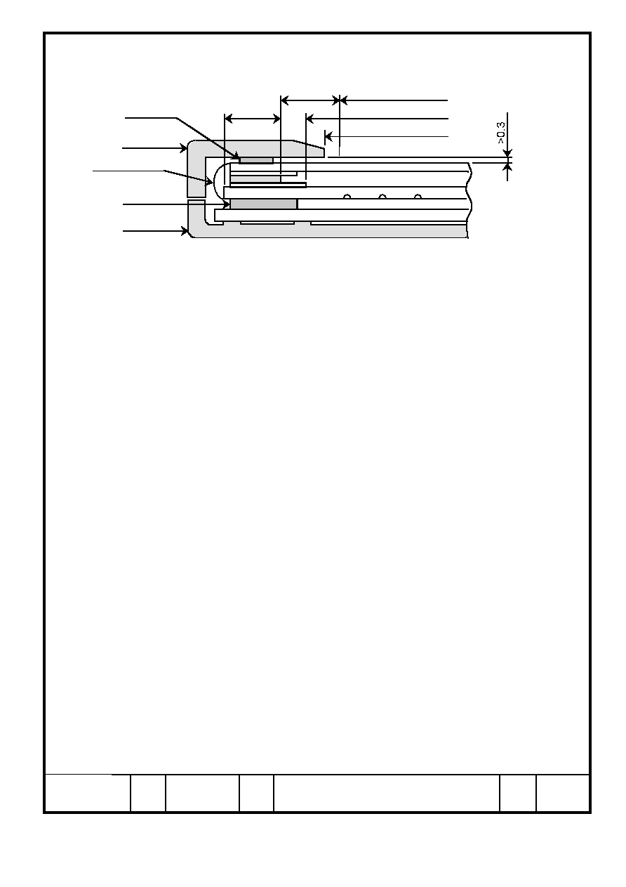
(5) The clearance betw een the touch panel and the case shall be designed so that the case edge
never presses the input screen w hen it is deformed by heat or other causes.
(6) The case shall be designed not to touch the tail portion (FPC for touch panel).
(4) When assembling the touch panel and your case, please refer to the figure below .
LCM
Case
Tape
Touch panel
Case
Cushion
Insulated area
(>2.0)
Effective area
Transparent area
Case opening

3284PS 2711 - SX21V001-Z4A - 3
June 10, '99
11-3/4
Displays,
Hitachi, Ltd.
Sh.
No.
Page
Date
(3) Lightly w ipe to clean the dirty surface w ith absorbent cotton or other sof t material like chamois,
soaked in the recommended chemicals w ithout scrubbing it hardly.
Alw ays w ipe the surface horizontally or vertically. Never give a w ipe in a circle. To prevent
the display surface from damage and keep the appearance in good state, it is sufficient, in general,
to w ipe it w ith absorbent cotton.
(4) Immediately w ipe off saliva or w ater drop attached on the display area because it may cause
def ormation or faded color.
(5) Fogy dew deposited on the surface may cause a damage, stain or dirt to the polarizer.
When you need to take out the LCD module from some place at low temperature for test, etc.
It is required to be w armed them up to be temperature higher than room temperature before taking
them out.
(6) Touching the display area or I/F pins w ith bare hands or contaminating them are prohibited,
because the stain on the display area and poor insulation betw een terminals are often caused by
being touched w ith bare hands.
(Some cosmetics are detrimental to polarizers.)
(7) In general, the glass is fragile so that it, especially on its periphery, tends to be cracked or
chipped in handling. Please do not give the LCD module sharp shocks caused by falling etc.
(8) Maximum pressure to the surface must be less than 1.96
×
10
4
Pa (0.2kgf /cm
2
).
And if the pressure area is less than 1cm
2
, maximum pressure must be less than 1.96N (0.2kgf).
(9) Since the metal w idth is narrow on these locations (see page 9-1/2), please be careful w ith
handling.
(10) Top sheets shall be cleaned gently using a sof t cloth such as those used f or glasses.
Hard w iping accumulated dust w ill leave scars on the surface even using a cloth.
11.5 OPERATION PRECAUTION
(1) Using a LCM module beyond its maximum ratings may result in its permanent destruction.
LCM module's should usually be used under recommended operating conditions show n in
chapter 5. Exceeding any of these conditions may adversely affect its reliability.
(2) Response time w ill be extremely delayed at low er temperature than the specif ied operating
temperature range and on the other hand LCD's show s dark blue color at higher temperature.
How ever those phenomena do not mean def ects of the LCD module. Those phenomena w ill
disappear in the specified operating temperature range.
(3) If the display area is pushed hard during operation, some display patterns w ill be abnormally
displayed.

3284PS 2711 - SX21V001-Z4A - 3
June 10, '99
11-4/4
Displays,
Hitachi, Ltd.
Sh.
No.
Page
Date
(4) A slight dew depositing on terminals may cause electrochemical reaction w hich leads to terminal
open circuit. Please operate the LCD module under the relative condition of 40
°
C 85%RH.
(5) Resistance renge : Your controller shall be set up to allow the resistance range of touch panel
specified in our CAS.
(6) Pointed position of touch panel may shift ow ing to a change in resistance of touch panel
depending on the operation condition. To compensate this shif t, the set shall be given a calibration
function.
(7) Input shall be made w ith a stylus pen (polyacetal, R0.8). Chances are very high that use of a
metal piece including a ball point pen or sharp edge w ill impair accuracy.
(8) The touch panel is an auxiliary input device. The system shall be designed to have other input
device.
11.6 STORAGE
In case of storing LCD module for a long period of time (for instance, for years) for the purpose of
replacement use, the follow ing precautions necessary.
(1) Store the LCD modules in a dark place ; do not expose them to sunlight or ultraviolet rays.
(2) Keep the temperature betw een 10
°
C and 35
°
C at normal humidity.
(3) Store the LCD modules in the container w hich is used for shipping from us.
(4) No articles shall be lef t on the surface over an extended period of time.
11.7 SAFETY
The LCD modules include Cold Cathode Fluorescent Lamp (CFL). CFL contains a small amount of
mercury. Please follow local ordinances or regulations for disposal.
Wear finger cots or gloves w henever handling or assembling a touch panel because its glass
edges are sharp.

3284PS 2712 - SX21V001-Z4A - 3
June 10, '99
12-1/2
12.1 LOT MARK
Lot mark is consisted of 4 digits f or production lot and
6 or 7 digits f or production control.
12. DESIGNATION OF LOT MARK
Year
Figure in
lot mark
1999
2000
2001
2002
2
1
0
9
9
0
4
2
Week
Month
Year
Digits for production control
Week
Figure in
lot mark
1
7
4
3
2
1
(day in Calender)
5
8
14
15
21
22
28
29
31
Month
Figure in
lot mark
Jan.
01
Month
Figure in
lot mark
Feb.
02
Mar.
03
Apr .
04
May
05
June
06
July
07
Aug.
08
Sep.
09
Oct.
10
Nov.
11
Dec.
12
Displays,
Hitachi, Ltd.
Sh.
No.
Page
Date

3284PS 2712 - SX21V001-Z4A - 3
June 10, '99
12-2/2
12.2 REVISION
REV No.
ITEM
LOT No.
PRODUCTION CONTROL No.
A
00001
12.3 LOCATION OF LOT MARK
Either Label A or Label B is being attached on the back side of LCM.
Label A
Note 1 : JAPAN or TAIWAN
SX21V001-Z4A
9042TN00001
WARNING HIGH VOLTAGE
REV.
MADE IN
Lot No.
Production Control No.
Rev No.
Note 1
Label B
SX21V001-Z4A
9042TN00001
REV.
MADE IN
Lot No.
Production
Control No.
Rev No.
Note 1
WARNING HIGH VOLTAGE
52 00 0H 6 K 1 1 200001
Displays,
Hitachi, Ltd.
Sh.
No.
Page
Date
B
Changed PCB

3284PS 2713 - SX21V001-Z4A - 3
June 10, '99
13-1/1
13. PRECAUTION FOR USE
(1) A limit sample should be provided by the both parities on an occasion w hen the both parties
agree to its necessity.
Judgment by a limit sample shall take effect af ter the limit sample has been established and
confirmed by the both parties.
(2) On the f ollow ing occasions, the handling of the problem should be decided through
discussion and agreement betw een responsible persons of the both parties.
(1) When a question is arisen in the specifications.
(2) When a new problem is arisen w hich is not specif ied in the specifications.
(3) When an inspection specif ication change or operating condition change by customer
is reported to HITACHI, and some problem is arisen in the specif ication due to the
change.
(4) When a new problem is arisen at the customer's operating set for sample evaluation
(3) Regarding the treatment for maintenance and repairing, both parties w ill discuss it in six month
later after latest delivery of this product.
The precaution that should be observed w hen handling LCM have been explained above.
If any points are unclear or if you have any requests, please contact Hitachi.
Displays,
Hitachi, Ltd.
Sh.
No.
Page
Date