 | –≠–ª–µ–∫—Ç—Ä–æ–Ω–Ω—ã–π –∫–æ–º–ø–æ–Ω–µ–Ω—Ç: HMC265 | –°–∫–∞—á–∞—Ç—å:  PDF PDF  ZIP ZIP |
MICROWAVE CORPORATION
5 - 58
For price, delivery, and to place orders, please contact Hittite Microwave Corporation:
12 Elizabeth Drive, Chelmsford, MA 01824 Phone: 978-250-3343 Fax: 978-250-3373
Order Online at www.hittite.com
MIXERS - CHIP
5
HMC265
v01.0701
General Description
Features
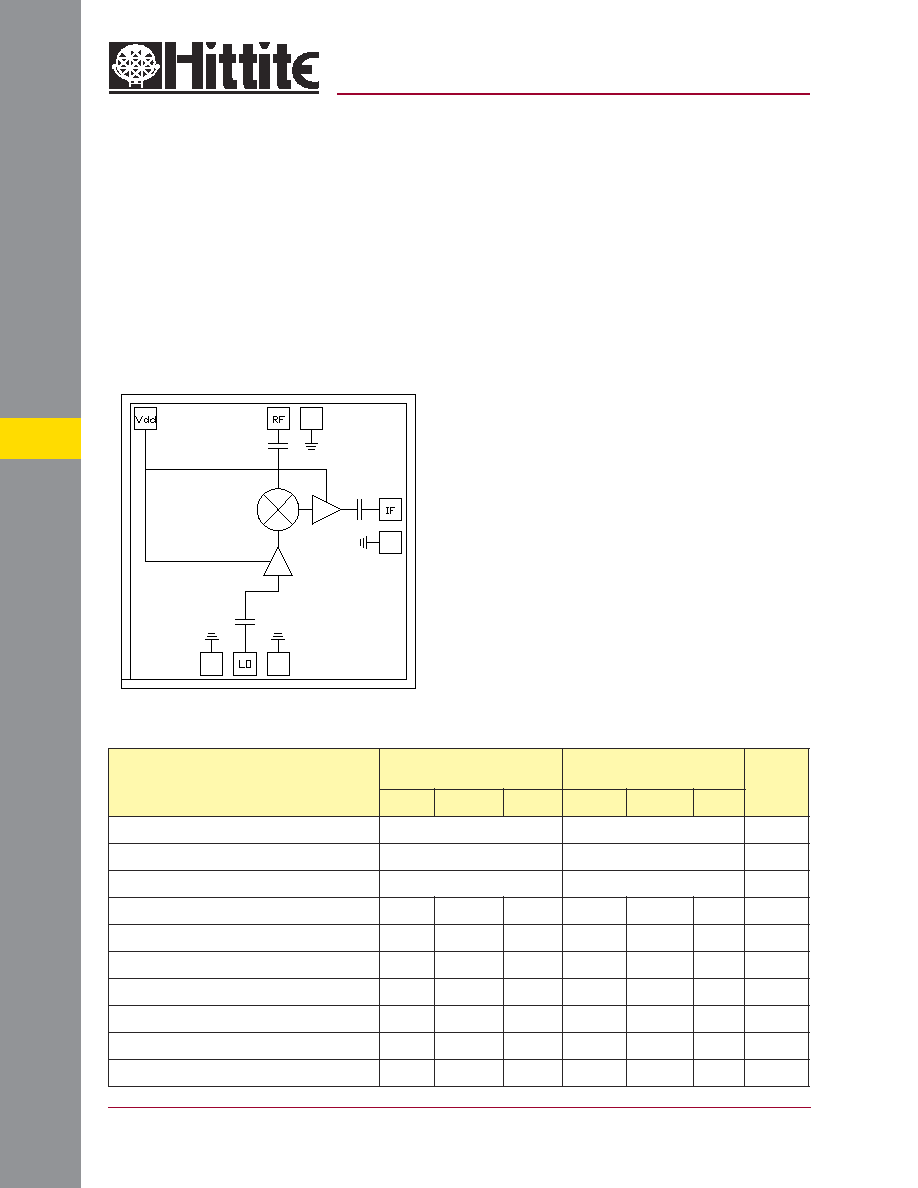
Functional Diagram
Integrated LO Amplifi er: -4 dBm Input
Sub-Harmonically Pumped (x2) LO
Integrated IF Amplifi er: 3 dB Gain
Small Size: 1.32mm x 1.32mm
Electrical Specifi cations,
T
A
= +25∞ C, LO Drive = -4 dBm
Typical Applications
The HMC265 is ideal for:
∑ Microwave Point to Point Radios
∑ LMDS
∑ SATCOM
The HMC265 chip is a sub-harmonically pumped
(x2) MMIC downconverter with integrated LO & IF
amplifi ers. The chip utilizes a GaAs PHEMT tech-
nology that results in a small overall chip area of
1.74 mm
2
. The 2LO to RF isolation is excellent
eliminating the need for additional fi ltering. The
LO amplifi er is a single bias (+3V to +4V) two
stage design with only -4 dBm nominal drive
requirement. All data is with the chip in a 50
ohm test fi xture connected via 0.025 mm (1 mil)
diameter wire bonds of minimal length <0.31 mm
(<12 mils). This downconverter IC is an excellent,
smaller, and more reliable replacement to hybrid
diode based downconverter MMIC assemblies.
GaAs MMIC SUB-HARMONICALLY
PUMPED DOWNCONVERTER, 20 - 32 GHz
Parameter
IF = 1 GHz
Vdd = +4V
IF = 1 GHz
Vdd = +4V
Units
Min.
Typ.
Max.
Min.
Typ.
Max.
Frequency Range, RF
20 - 32
27 - 30
GHz
Frequency Range, LO
10 - 16
13.5 - 15
GHz
Frequency Range, IF
0.7 - 3.0
0.7 - 3.0
GHz
Conversion Gain (RF to IF)
-2
3
7
-2
2
5
dB
Noise Figure (SSB)
13
13
dB
2LO to RF Isolation
17
20 ~ 40
28
35
dB
2LO to IF Isolation
40
50 ~ 60
45
55
dB
IP3 (Input)
2
10
9
13
dBm
1 dB Compression (Input)
-5
2
-2
2
dBm
Supply Current (Idd)
50
50
mA

MICROWAVE CORPORATION
5 - 59
For price, delivery, and to place orders, please contact Hittite Microwave Corporation:
12 Elizabeth Drive, Chelmsford, MA 01824 Phone: 978-250-3343 Fax: 978-250-3373
Order Online at www.hittite.com
MIXERS - CHIP
5
v01.0701
-20
-15
-10
-5
0
5
10
18
20
22
24
26
28
30
32
34
CONVERSION GAIN (dB)
RF FREQUENCY (GHz)
+85 C
-55 C
+25 C
-20
-15
-10
-5
0
5
10
18
20
22
24
26
28
30
32
34
CONVERSION GAIN (dB)
RF FREQUENCY (GHz)
+85 C
-55 C
+25 C
Conversion Gain vs. Temperature
@ LO = -4 dBm Vdd = +4V
HMC265
-20
-15
-10
-5
0
5
10
18
20
22
24
26
28
30
32
34
CONVERSION GAIN (dB)
RF FREQUENCY (GHz)
-4dBm
-8dBm
-6dBm
-2dBm
0dBm
-70
-60
-50
-40
-30
-20
-10
0
10
18
20
22
24
26
28
30
32
34
ISOLATION (dB)
RF FREQUENCY (GHz)
LO/IF
RF/IF
LO/RF
2LO/RF
2LO/IF
-20
-15
-10
-5
0
5
10
18
20
22
24
26
28
30
32
34
CONVERSION GAIN (dB)
RF FREQUENCY (GHz)
-4dBm
-6dBm
-2dBm
-70
-60
-50
-40
-30
-20
-10
0
10
18
20
22
24
26
28
30
32
34
ISOLATION (dB)
RF FREQUENCY (GHz)
RF/IF
LO/IF
LO/RF
2LO/RF
2LO/IF
Conversion Gain vs. Temperature
@ LO = -4 dBm Vdd = +3V
Conversion Gain vs. LO Drive
@ Vdd = +4V
Conversion Gain vs. LO Drive
@ Vdd = +3V
Isolation @ LO = -4 dBm, Vdd = +4V
Isolation @ LO = -4 dBm, Vdd = +3V
GaAs MMIC SUB-HARMONICALLY
PUMPED DOWNCONVERTER, 20 - 32 GHz

MICROWAVE CORPORATION
5 - 60
For price, delivery, and to place orders, please contact Hittite Microwave Corporation:
12 Elizabeth Drive, Chelmsford, MA 01824 Phone: 978-250-3343 Fax: 978-250-3373
Order Online at www.hittite.com
MIXERS - CHIP
5
v01.0701
HMC265
0
2
4
6
8
10
12
14
16
18
20
18
20
22
24
26
28
30
32
34
THIRD ORDER INTERCEPT (dBm)
RF FREQUENCY (GHz)
-4 dBm
-6 dBm
-2 dBm
0
2
4
6
8
10
12
14
16
18
20
18
20
22
24
26
28
30
32
34
THIRD ORDER INTERCEPT (dBm)
RF FREQUENCY (GHz)
-55C
+25C
+85C
IP3 vs. LO Drive @ Vdd = +4V
IP3 vs. Temperature
@ LO = -4 dBm, Vdd = +4V
LO & RF Return Loss
@ LO = -4 dBm, Vdd = +4V
-20
-15
-10
-5
0
0
5
10
15
20
25
30
35
40
RETURN LOSS (dB)
FREQUENCY (GHz)
RF
LO
GaAs MMIC SUB-HARMONICALLY
PUMPED DOWNCONVERTER, 20 - 32 GHz
IF Return Loss
@ LO = -4 dBm, Vdd = +4V
P1dB vs. Temperature
@ LO = -4 dBm, Vdd = +4V
IF Bandwidth @ LO = -4 dBm
-20
-15
-10
-5
0
0
1
2
3
4
5
6
RETURN LOSS (dB)
FREQUENCY (GHz)
IF
-5
-4
-3
-2
-1
0
1
2
3
18
20
22
24
26
28
30
32
34
P1dB (dBm)
RF FREQUENCY (GHz)
+25 C
+85 C
-55 C
-20
-15
-10
-5
0
5
10
0
1
2
3
4
5
6
IF CONVERSION GAIN (dB)
IF FREQUENCY (GHz)
Vdd = +4V
Vdd = +3V
MICROWAVE CORPORATION
5 - 61
For price, delivery, and to place orders, please contact Hittite Microwave Corporation:
12 Elizabeth Drive, Chelmsford, MA 01824 Phone: 978-250-3343 Fax: 978-250-3373
Order Online at www.hittite.com
MIXERS - CHIP
5
v01.0701
HMC265
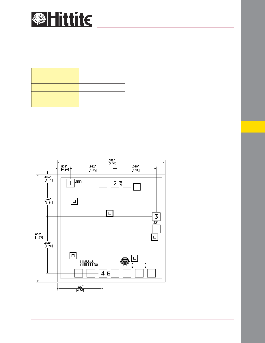
Outline Drawing
(See Handling Mounting Bonding Note)
Absolute Maximum Ratings
GaAs MMIC SUB-HARMONICALLY
PUMPED DOWNCONVERTER, 20 - 32 GHz
RF / IF Input (Vdd = +4V)
+13 dBm
LO Drive (Vdd = +4V)
+13 dBm
Vdd
+5.5 Vdc
Storage Temperature
-65 to +150 ∞C
Operating Temperature
-55 to +85 ∞C
NOTES:
1. ALL DIMENSIONS ARE IN INCHES [MM].
2. DIE THICKNESS IS .004".
3. TYPICAL BOND PAD IS .004" SQUARE.
4. BOND PAD SPACING CENTER TO
CENTER IS .006".
5. BACKSIDE METALLIZATION: GOLD.
6. BOND PAD METALLIZATION: GOLD.
7. BACKSIDE METAL IS GROUND.
8. CONNECTION NOT REQUIRED FOR
UNLABELED BOND PADS.

MICROWAVE CORPORATION
5 - 62
For price, delivery, and to place orders, please contact Hittite Microwave Corporation:
12 Elizabeth Drive, Chelmsford, MA 01824 Phone: 978-250-3343 Fax: 978-250-3373
Order Online at www.hittite.com
MIXERS - CHIP
5
MIC Assembly Techniques
Mounting & Bonding Techiniques for Millimeterwave GaAs MMICs
The die should be attached directly to the ground plane eutectically or with conductive epoxy (see HMC general Handling, Mounting,
Bonding Note).
50 Ohm Microstrip transmission lines on 0.127mm (5 mil) thick alumina thin fi lm
substrates are recommended for bringing RF to and from the chip (Figure 1). If
0.254mm (10 mil) thick alumina thin fi lm substrates must be used, the die should
be raised 0.150mm (6 mils) so that the surface of the die is coplanar with the
surface of the substrate. One way to accomplish this is to attach the 0.102mm
(4 mil) thick die to a 0.150mm (6 mil) thick molybdenum heat spreader (moly-tab)
which is then attached to the ground plane (Figure 2).
Microstrip substrates should be brought as close to the die as possible in order
to minimize bond wire length. Typical die-to-substrate spacing is 0.076mm (3
mils).
An RF bypass capacitor should be used on the Vdd input. A 100 pF single layer
capacitor (mounted eutectically or by conductive epoxy) placed no further than
0.762mm (30 mils) from the chip is recommended. The photo in fi gure 3 shows a
typical assembly for the HMC265 MMIC chip.
HMC265
v01.0701
GaAs MMIC SUB-HARMONICALLY
PUMPED DOWNCONVERTER, 20 - 32 GHz
Figure 3: Typical HMC265 Assembly