 | ÐлекÑÑоннÑй компоненÑ: HMC383 | СкаÑаÑÑ:  PDF PDF  ZIP ZIP |
1_amplifier_chip_section.indd
1
A
M
P
L
IF
IE
RS
-
C
H
IP
1 - 26
For price, delivery, and to place orders, please contact Hittite Microwave Corporation:
20 Alpha Road, Chelmsford, MA 01824 Phone: 978-250-3343 Fax: 978-250-3373
Order On-line at www.hittite.com
HMC383
GaAs PHEMT MMIC MEDIUM POWER
AMPLIFIER, 12 - 30 GHz
v00.0305
General Description
Features
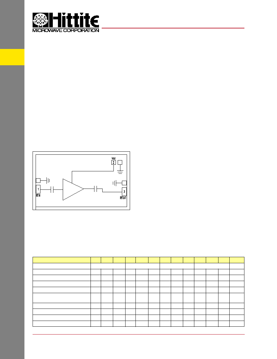
Functional Diagram
The HMC383 is a general purpose GaAs PHEMT
MMIC Driver Amplifi er which operates between
12 and 30 GHz. The amplifi er provides 16 dB
of gain and +18 dBm of saturated power from
a +5.0 V supply voltage. Consistent gain and
output power across the operating band make
it possible to use a common driver/LO amplifi er
approach in multiple radio bands. The HMC383
amplifi er can easily be integrated into Multi-Chip-
Modules (MCMs) due to its small (2.62mm
2
)
size. The backside of the die is both RF and DC
ground, simplifying the assembly process and
reducing performance variation. All data is tested
with the chip in a 50 Ohm test fi xture connected
via 0.025mm (1 mil) diameter wire bonds of
minimal length 0.31mm (12 mils).
Gain: 16 dB
Saturated Output Power: +18 dBm
Output IP3: +25 dBm
Single Supply Voltage: +5.0 V @ 101 mA
50 Ohm Matched Input/Output
Electrical Specifi cations,
T
A
= +25° C, Vdd = +5V
Typical Applications
The HMC383 is ideal for use as a driver amplifi er
for:
· Point-to-Point Radios
· Point-to-Multi-Point Radios & VSAT
· Test Equipment & Sensors
· LO Driver for HMC Mixers
· Military & Space
Parameter
Min.
Typ.
Max.
Min.
Typ.
Max.
Min.
Typ.
Max.
Min.
Typ.
Max.
Units
Frequency Range
12 - 18
18 - 24
24 - 28
28 - 30
GHz
Gain
13
16
14
17
13
16
12
15
dB
Gain Variation Over Temperature
0.03
0.04
0.03
0.04
0.03
0.04
0.03
0.04
dB/ °C
Input Return Loss
14
12
14
7
dB
Output Return Loss
13
12
7
5
dB
Output Power for 1 dB Compression
(P1dB)
12
15
13.5
16.5
13
16
13
16
dBm
Saturated Output Power (Psat)
18
18
17
18
dBm
Output Third Order Intercept (IP3)
25
25
24
23
dBm
Noise Figure
9
7
6.5
7.5
dB
Supply Current (Idd)
101
101
101
101
mA
1
A
M
P
L
IF
IE
RS
-
C
H
IP
1 - 27
For price, delivery, and to place orders, please contact Hittite Microwave Corporation:
20 Alpha Road, Chelmsford, MA 01824 Phone: 978-250-3343 Fax: 978-250-3373
Order On-line at www.hittite.com
HMC383
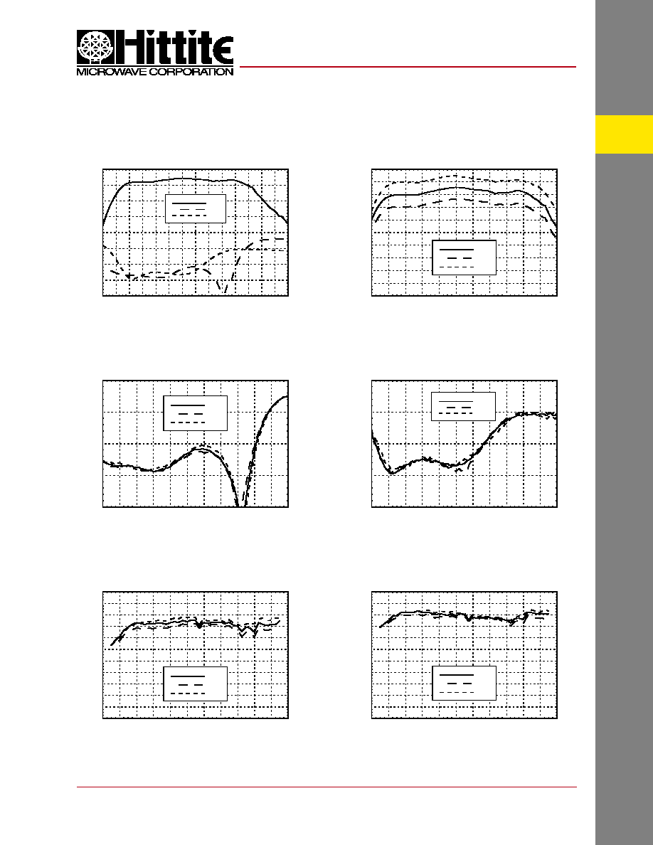
Input Return Loss vs. Temperature
Output Return Loss vs. Temperature
Broadband Gain & Return Loss
Gain vs. Temperature
P1dB vs. Temperature
Psat vs. Temperature
v00.0305
-20
-15
-10
-5
0
5
10
15
20
8
10 12 14 16 18 20 22 24 26 28 30 32 34 36
S21
S11
S22
RESPONSE (dB)
FREQUENCY (GHz)
-20
-15
-10
-5
0
10
12
14
16
18
20
22
24
26
28
30
32
+25C
+85C
-55C
RETURN LOSS (dB)
FREQUENCY (GHz)
-20
-15
-10
-5
0
10
12
14
16
18
20
22
24
26
28
30
32
+25C
+85C
-55C
RETURN LOSS (dB)
FREQUENCY (GHz)
0
2
4
6
8
10
12
14
16
18
20
22
10
12
14
16
18
20
22
24
26
28
30
32
+25C
+85C
-55C
Psat (dBm)
FREQUENCY (GHz)
0
2
4
6
8
10
12
14
16
18
20
22
10
12
14
16
18
20
22
24
26
28
30
32
+25C
+85C
-55C
P1dB (dBm)
FREQUENCY (GHz)
0
2
4
6
8
10
12
14
16
18
20
10
12
14
16
18
20
22
24
26
28
30
32
+25C
+85C
-55C
GAIN
(dB)
FREQUENCY (GHz)
GaAs PHEMT MMIC MEDIUM POWER
AMPLIFIER, 12 - 30 GHz
1
A
M
P
L
IF
IE
RS
-
C
H
IP
1 - 28
For price, delivery, and to place orders, please contact Hittite Microwave Corporation:
20 Alpha Road, Chelmsford, MA 01824 Phone: 978-250-3343 Fax: 978-250-3373
Order On-line at www.hittite.com
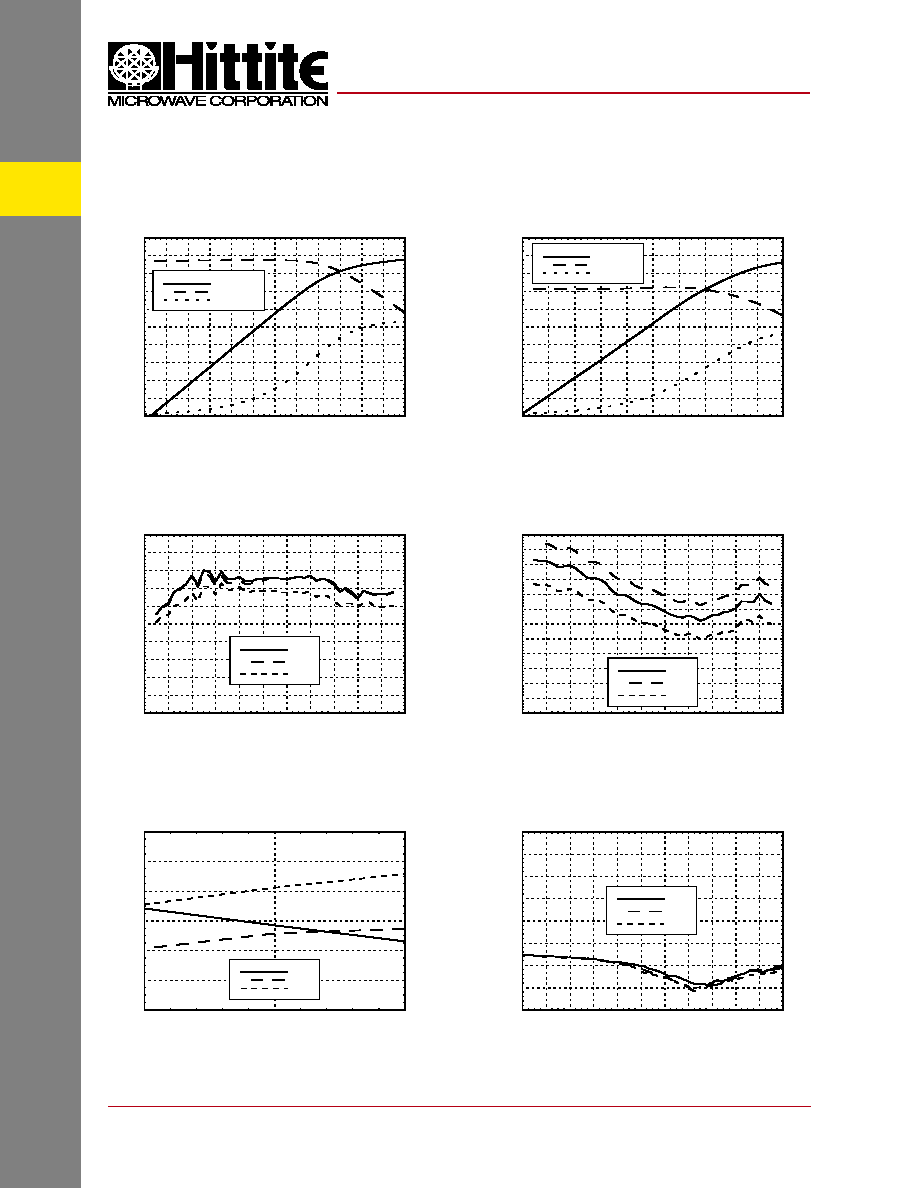
Power Compression @ 18 GHz
Output IP3 vs. Temperature
Noise Figure vs. Temperature
Gain & Power vs. Supply Voltage @ 18 GHz
Reverse Isolation vs. Temperature
Power Compression @ 30 GHz
HMC383
v00.0305
0
1
2
3
4
5
6
7
8
9
10
11
12
10
12
14
16
18
20
22
24
26
28
30
32
+25C
+85C
-55C
NOI
SE FI
GURE (dB)
FREQUENCY (GHz)
10
12
14
16
18
20
22
24
26
28
30
10
12
14
16
18
20
22
24
26
28
30
32
+25C
+85C
-55C
OIP3 (dBm)
FREQUENCY (GHz)
-80
-70
-60
-50
-40
-30
-20
-10
0
10
12
14
16
18
20
22
24
26
28
30
32
+25C
+85C
-55C
ISOLATION (dB)
FREQUENCY (GHz)
14
15
16
17
18
19
20
4.5
5
5.5
Gain
P1dB
Psat
GAIN (dB), P1dB (d
Bm), Psat (dBm)
Vdd Supply Voltage (Vdc)
0
2
4
6
8
10
12
14
16
18
20
-14
-12
-10
-8
-6
-4
-2
0
2
4
6
Pout (dBm)
Gain (dB)
PAE (%)
Pout (dBm), GAIN (dB), PAE (%)
INPUT POWER (dBm)
0
2
4
6
8
10
12
14
16
18
20
-18 -16 -14 -12 -10
-8
-6
-4
-2
0
2
4
6
Pout (dBm)
Gain (dB)
PAE (%)
Pout (dBm), GAIN (dB), PAE (%)
INPUT POWER (dBm)
GaAs PHEMT MMIC MEDIUM POWER
AMPLIFIER, 12 - 30 GHz
1
A
M
P
L
IF
IE
RS
-
C
H
IP
1 - 29
For price, delivery, and to place orders, please contact Hittite Microwave Corporation:
20 Alpha Road, Chelmsford, MA 01824 Phone: 978-250-3343 Fax: 978-250-3373
Order On-line at www.hittite.com
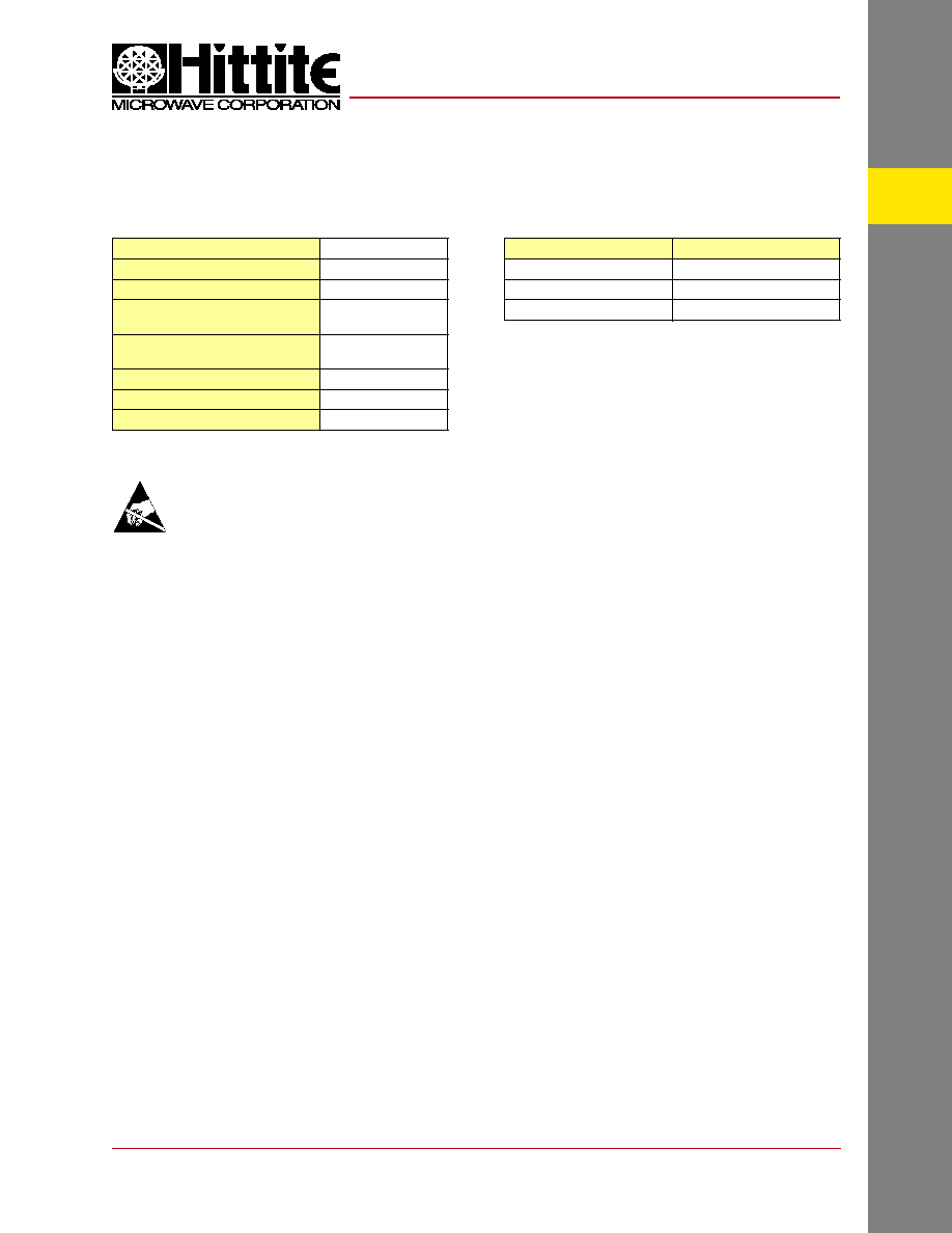
Absolute Maximum Ratings
Drain Bias Voltage (Vdd)
+5.5 Vdc
RF Input Power (RFin)(Vdd = +5.0 Vdc)
+10 dBm
Channel Temperature
175 °C
Continuous Pdiss (T= 85 °C)
(derate 12 mW/°C above 85 °C)
1.1 W
Thermal Resistance
(channel to die bottom)
82 °C/W
Storage Temperature
-65 to +150 °C
Operating Temperature
-55 to +85 °C
ESD Sensitivity (HBM)
Class 1A
Vdd (V)
Idd (mA)
+4.5
100
+5.0
101
+5.5
102
Typical Supply Current vs. Vdd
Note: Amplifi er will operate over full voltage ranges shown above
ELECTROSTATIC SENSITIVE DEVICE
OBSERVE HANDLING PRECAUTIONS
HMC383
v00.0305
GaAs PHEMT MMIC MEDIUM POWER
AMPLIFIER, 12 - 30 GHz
1
A
M
P
L
IF
IE
RS
-
C
H
IP
1 - 30
For price, delivery, and to place orders, please contact Hittite Microwave Corporation:
20 Alpha Road, Chelmsford, MA 01824 Phone: 978-250-3343 Fax: 978-250-3373
Order On-line at www.hittite.com
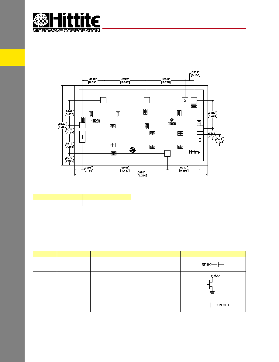
Pad Descriptions
Pad Number
Function
Description
Interface Schematic
1
RF IN
This pad is AC coupled and matched to 50 Ohms from
12 - 30 GHz.
2
Vdd
Power Supply Voltage for the amplifi er. External bypass
capacitors of 100 pF and 0.1 µF are required.
3
RF OUT
This pad is AC coupled and matched to 50 Ohms from
12 - 30 GHz.
Outline Drawing
Die Packaging Information
[1]
Standard
Alternate
GP-1
[2]
[1] Refer to the "Packaging Information" section for die
packaging dimensions.
[2] For alternate packaging information contact Hittite
Microwave Corporation.
HMC383
v00.0305
NOTES:
1. ALL DIMENSIONS ARE IN INCHES [MM]
2. DIE THICKNESS IS .004"
3. TYPICAL BOND PAD IS .004" SQUARE
4. BACKSIDE METALLIZATION: GOLD
5. BOND PAD METALLIZATION: GOLD
6. BACKSIDE METAL IS GROUND.
7. CONNECTION NOT REQUIRED FOR UNLABELED BOND PADS.
8. OVERALL DIE SIZE ± .002
GaAs PHEMT MMIC MEDIUM POWER
AMPLIFIER, 12 - 30 GHz