
8
A
M
P
L
IF
IE
RS
-
S
M
T
8 - 208
For price, delivery, and to place orders, please contact Hittite Microwave Corporation:
20 Alpha Road, Chelmsford, MA 01824 Phone: 978-250-3343 Fax: 978-250-3373
Order On-line at www.hittite.com
HMC441LH5
GaAs PHEMT MMIC MEDIUM
POWER AMPLIFIER, 7.0 - 15.5 GHz
v00.0705
General Description
Features
Functional Diagram
The HMC441LH5 is a broadband 7 to 15.5 GHz
GaAs PHEMT MMIC Medium Power Amplifi er housed
in a hermetic SMT leadless package. The amplifi er
provides 15 dB of gain and 21.5 dBm of saturated
power at 25% PAE from a +5.0V supply. This 50
Ohm matched amplifi er does not require any external
components, and the RF I/Os are DC blocked,
making it an ideal linear gain block or driver amplifi er.
The HMC441LH5 allows the use of surface mount
manufacturing techniques and is suitable for high
reliability military, industrial & space applications.
Gain: 15 dB
Saturated Power: +21.5 dBm @ 25% PAE
Single Positive Supply: +5.0 V
50 Ohms Matched Input/Output
Hermetic SMT Package, 25mm
2
Screening to MIL-PRF-38535 (Class B or S) Available
Electrical Specifications,
T
A
= +25� C, Vdd = 5V
Typical Applications
Parameter
Min.
Typ.
Max.
Min.
Typ.
Max.
Min.
Typ.
Max.
Min.
Typ.
Max.
Units
Frequency Range
7.0 - 8.0
8.0 - 13.0
13.0 - 14.0
14.0 - 15.5
GHz
Gain
11
14
13
16
12
15
10.5
13.5
dB
Gain Variation Over Temperature
0.015
0.02
0.015
0.02
0.015
0.02
0.015
0.02
dB/ �C
Input Return Loss
11
13
10
8
dB
Output Return Loss
10
15
14
12
dB
Output Power for 1 dB
Compression (P1dB)
15.5
18.5
17
20
16
19
16
19
dBm
Saturated Output Power (Psat)
20
21
21.5
21
dBm
Output Third Order Intercept (IP3)
30
32
32
32
dBm
Noise Figure
5.0
4.75
4.75
5.0
dB
Supply Current (Idd)
90
90
90
90
mA
The HMC441LH5 is a medium PA for:
� Telecom Infrastructure
� Military Radio, Radar & ECM
� Space Systems
� Test Instrumentation
8
A
M
P
L
IF
IE
RS
-
S
M
T
8 - 209
For price, delivery, and to place orders, please contact Hittite Microwave Corporation:
20 Alpha Road, Chelmsford, MA 01824 Phone: 978-250-3343 Fax: 978-250-3373
Order On-line at www.hittite.com
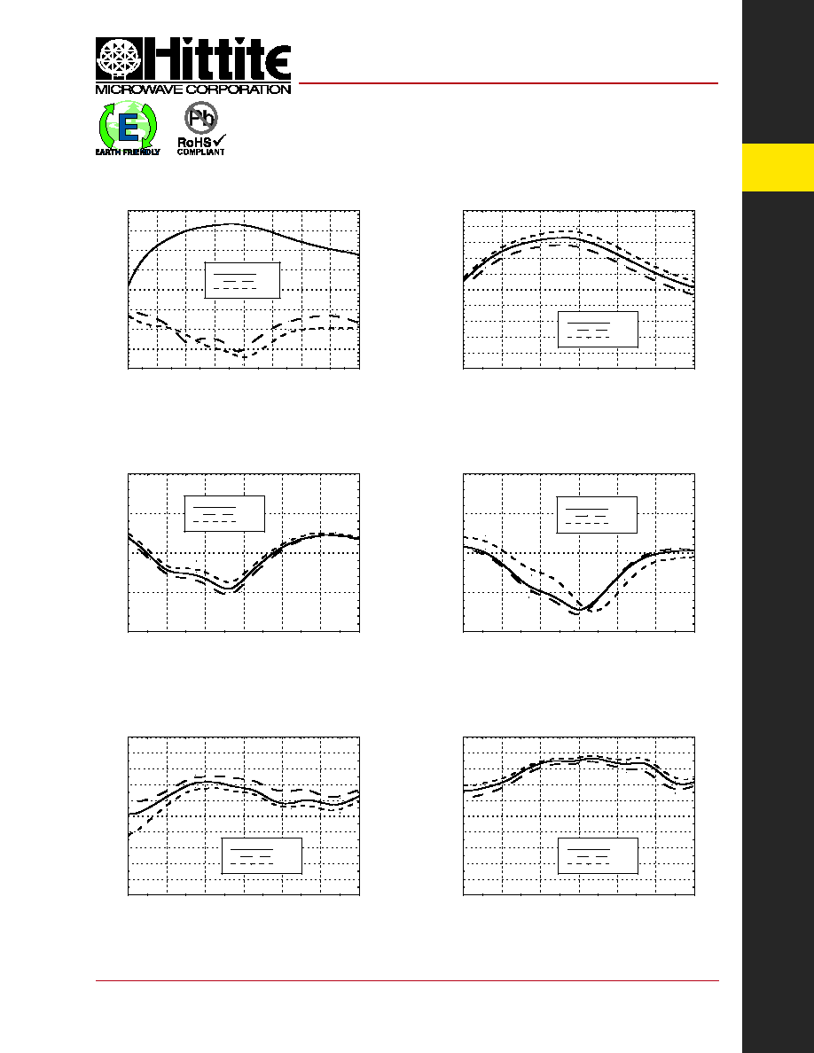
Input Return Loss vs. Temperature
Output Return Loss vs. Temperature
Broadband Gain & Return Loss
Gain vs. Temperature
P1dB vs. Temperature
Psat vs. Temperature
-20
-15
-10
-5
0
5
10
15
20
4
6
8
10
12
14
16
18
20
S21
S11
S22
RESPONSE (dB)
FREQUENCY (GHz)
HMC441LH5
GaAs PHEMT MMIC MEDIUM
POWER AMPLIFIER, 7.0 - 15.5 GHz
v00.0705
13
14
15
16
17
18
19
20
21
22
23
6
8
10
12
14
16
18
+25C
+85C
-40C
Psat (dBm)
FREQUENCY (GHz)
13
14
15
16
17
18
19
20
21
22
23
6
8
10
12
14
16
18
+25C
+85C
-40C
P1dB (dBm)
FREQUENCY (GHz)
-20
-15
-10
-5
0
6
8
10
12
14
16
18
+25C
+85C
-40C
RETURN LOSS (dB)
FREQUENCY (GHz)
-20
-15
-10
-5
0
6
8
10
12
14
16
18
+25C
+85C
-40C
RETURN LOSS (dB)
FREQUENCY (GHz)
0
2
4
6
8
10
12
14
16
18
20
6
8
10
12
14
16
18
+25C
+85C
-40C
GAIN
(dB)
FREQUENCY (GHz)
8
A
M
P
L
IF
IE
RS
-
S
M
T
8 - 210
For price, delivery, and to place orders, please contact Hittite Microwave Corporation:
20 Alpha Road, Chelmsford, MA 01824 Phone: 978-250-3343 Fax: 978-250-3373
Order On-line at www.hittite.com
Power Compression @ 12 GHz
Output IP3 vs. Temperature
Noise Figure vs. Temperature
Gain, Power & OIP3
vs. Supply Voltage @ 12 GHz
Reverse Isolation vs. Temperature
HMC441LH5
GaAs PHEMT MMIC MEDIUM
POWER AMPLIFIER, 7.0 - 15.5 GHz
v00.0705
0
1
2
3
4
5
6
7
8
9
10
6
8
10
12
14
16
18
+25C
+85C
-40C
NOI
SE FI
GURE (dB)
FREQUENCY (GHz)
-50
-40
-30
-20
-10
0
6
8
10
12
14
16
18
+25C
+85C
-40C
ISOLATION (dB)
FREQUENCY (GHz)
14
16
18
20
22
24
26
28
30
32
34
36
4.5
4.6
4.7
4.8
4.9
5
5.1
5.2
5.3
5.4
5.5
Gain
P1dB
Psat
OIP3
GAIN (dB), P1dB (dBm),
Psat (dBm), OIP3 (dBm)
Vdd Supply Voltage (Vdc)
16
18
20
22
24
26
28
30
32
34
36
6
8
10
12
14
16
18
+25C
+85C
-40C
OIP3 (dBm)
FREQUENCY (GHz)
0
2
4
6
8
10
12
14
16
18
20
22
24
26
28
-10
-8
-6
-4
-2
0
2
4
6
8
10
Pout
Gain
PAE
Pout (dBm), GAIN (dB), PAE(%)
INPUT POWER (dBm)
8
A
M
P
L
IF
IE
RS
-
S
M
T
8 - 211
For price, delivery, and to place orders, please contact Hittite Microwave Corporation:
20 Alpha Road, Chelmsford, MA 01824 Phone: 978-250-3343 Fax: 978-250-3373
Order On-line at www.hittite.com
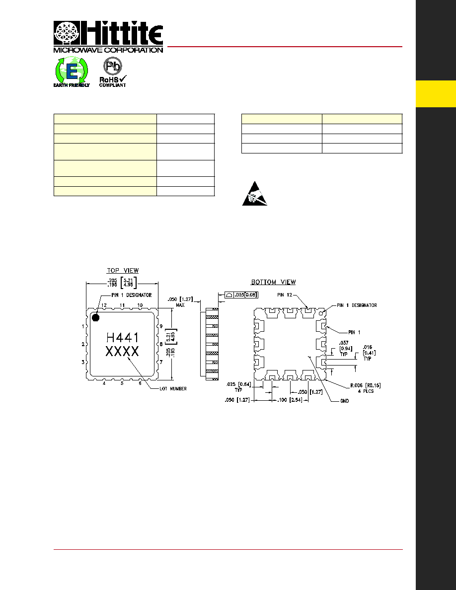
Outline Drawing
Absolute Maximum Ratings
Drain Bias Voltage (Vdd)
+6.0 Vdc
RF Input Power (RFin)(Vdd = +5.0 Vdc)
+15 dBm
Channel Temperature
175 �C
Continuous Pdiss (T = 85 �C)
(derate 6.9 mW/�C above 85 �C)
0.62 W
Thermal Resistance
(channel to ground paddle)
145 �C/W
Storage Temperature
-65 to +150 �C
Operating Temperature
-40 to +85 �C
Vdd (V)
Idd (mA)
+5.5
92
+5.0
90
+4.5
88
Note: Amplifi er will operate over full voltage range shown above
Typical Supply Current vs. Vdd
NOTES:
1. PACKAGE BODY MATERIAL: CERAMIC & KOVAR
2. LEAD AND GROUND PADDLE PLATING: GOLD 40 - 80 MICROINCHES.
3. DIMENSIONS ARE IN INCHES [MILLIMETERS].
4. LEAD SPACING TOLERANCE IS NON-CUMULATIVE
5. PAD BURR LENGTH 0.15mm MAX.
PAD BURR HEIGHT 0.25mm MAX.
6. ALL GROUND LEADS AND GROUND PADDLE MUST BE SOLDERED TO
PCB RF GROUND.
HMC441LH5
GaAs PHEMT MMIC MEDIUM
POWER AMPLIFIER, 7.0 - 15.5 GHz
v00.0705

8
A
M
P
L
IF
IE
RS
-
S
M
T
8 - 212
For price, delivery, and to place orders, please contact Hittite Microwave Corporation:
20 Alpha Road, Chelmsford, MA 01824 Phone: 978-250-3343 Fax: 978-250-3373
Order On-line at www.hittite.com
Pin Descriptions
Pin Number
Function
Description
Interface Schematic
1, 3-7, 9,
10, 12
GND
These pins and package bottom must be connected
to RF/DC ground.
2
RFIN
This pin is AC coupled and matched to 50 Ohms from
7.0 - 15.5 GHz.
8
RFOUT
This pin is AC coupled and matched to 50 Ohms from
7.0 - 15.5 GHz.
11
Vdd
Power Supply Voltage for the amplifi er. External bypass
capacitors are recommended.
HMC441LH5
GaAs PHEMT MMIC MEDIUM
POWER AMPLIFIER, 7.0 - 15.5 GHz
v00.0705
Application Circuit
Component
Value
C1
100 pF
C2
1,000 pF
C3
4.7 F

8
A
M
P
L
IF
IE
RS
-
S
M
T
8 - 213
For price, delivery, and to place orders, please contact Hittite Microwave Corporation:
20 Alpha Road, Chelmsford, MA 01824 Phone: 978-250-3343 Fax: 978-250-3373
Order On-line at www.hittite.com
Evaluation PCB
HMC441LH5
GaAs PHEMT MMIC MEDIUM
POWER AMPLIFIER, 7.0 - 15.5 GHz
v00.0705
The circuit board used in the fi nal application should
use RF circuit design techniques. Signal lines
should have 50 ohm impedance while the package
ground leads and exposed paddle should be con-
nected directly to the ground plane similar to that
shown. A suffi cient number of VIA holes should be
used to connect the top and bottom ground planes.
The evaluation circuit board shown is available from
Hittite upon request.
List of Material for Evaluation PCB 111560
[1]
Item
Description
J1 - J2
PCB Mount SMA RF Connector, SRI
U1
HMC441LH5
C1
100 pF Capacitor, 0402 Pkg.
C2
1,000 pF Capacitor, 0603 Pkg.
C3
4.7 F Capacitor, Tantalum
PCB
[2]
111558 Evaluation Board
[1] Reference this number when ordering complete evaluation PCB
[2] Circuit Board Material: Rogers 4350