 | ÐлекÑÑоннÑй компоненÑ: HMC500LP3 | СкаÑаÑÑ:  PDF PDF  ZIP ZIP |
Äîêóìåíòàöèÿ è îïèñàíèÿ www.docs.chipfind.ru
13
MOD
U
L
A
T
O
R
S
- SM
T
13 - 34
For price, delivery, and to place orders, please contact Hittite Microwave Corporation:
20 Alpha Road, Chelmsford, MA 01824 Phone: 978-250-3343 Fax: 978-250-3373
Order On-line at www.hittite.com
GaAs HBT VECTOR
MODULATOR 1.8 - 2.2 GHz
v01.0705
HMC500LP3
/
500LP3E
General Description
Features
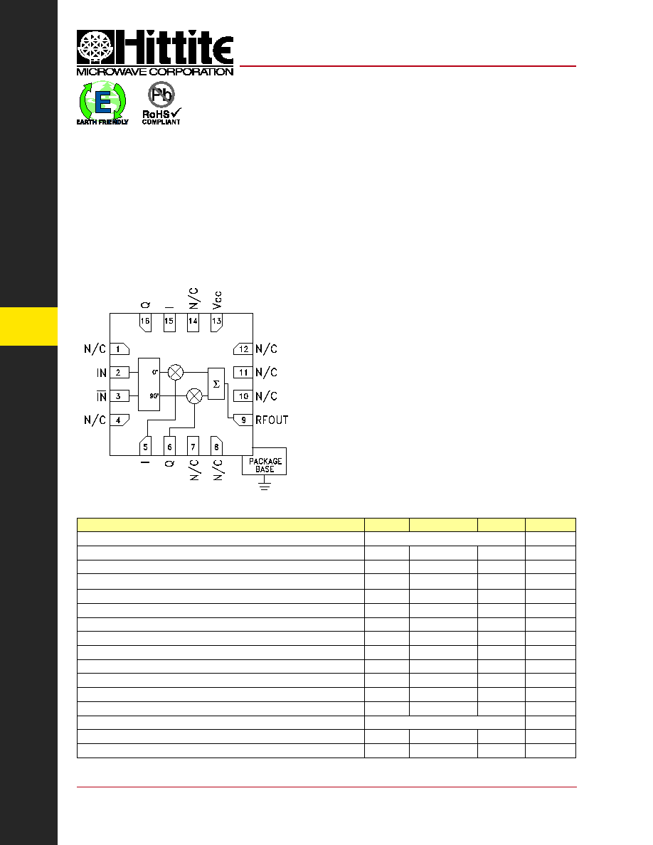
Functional Diagram
The HMC500LP3 & HMC500LP3E are high dynamic
range Vector Modulator RFICs which are targeted
for RF predistortion and feed-forward cancellation
circuits, as well as RF cancellation and beam forming
amplitude/phase correction circuits. The I & Q ports
of the HMC500LP3 & HMC500LP3E can be used
to continuously vary the phase and amplitude of RF
signals by up to 360 degrees and 40 dB respectively,
while supporting a 3 dB modulation bandwidth
of 150 MHz. With an input IP3 of +33 dBm and
input noise fl oor of -152 dBm/Hz (at -10 dB maximum
gain setting), the input IP3/noise fl oor ratio is 185 dB.
360° of Continuous Phase Control
40 dB of Continuous Gain Control
-162 dBm/Hz Output Noise Floor
+33 dBm Input IP3
3 x 3 mm QFN Plastic Package
Typical Applications
The HMC500LP3 / HMC500LP3E is ideal for:
· Wireless Infrastructure HPA &
MCPA
Error
Correction
· Pre-Distortion or Feed-Forward Linearization
· PCS, GSM and W-CDMA Systems
· Beam Forming or RF Cancellation Circuits
Electrical Specifications,
T
A
= +25° C, Vcc= +8V
Parameter
Min.
Typ.
Max.
Units
Frequency Range
1.8 - 2.2
GHz
Maximum Gain
-14
-10
dB
Gain Variation Over Temperature
0.012
0.02
dB / °C
Gain Flatness Across Any 60 MHz Bandwidth
0.15
dB
Gain Range
40
dB
Input Return Loss
17
dB
Output Return Loss
15
dB
Input Power for 1dB Compression (P1dB)
13
16
dBm
Input Third Order Intercept (IP3)
33
dBm
Output Noise
-162
dBm/Hz
Control Port Bandwidth (-3 dB)
150
MHz
Control Port Impedance
1.45k
Ohms
Control Port Capacitance
0.22
pF
Control Voltage Range
+0.5 to +2.5
Vdc
Group Delay Over 60 MHz Bandwidth
20
ps
Supply Current (Icq)
90
mA
Unless otherwise noted, measurements are made @ max. gain setting and 45° phase setting.
See application circuit for details.
13
MOD
U
L
A
T
O
R
S
- SM
T
13 - 35
For price, delivery, and to place orders, please contact Hittite Microwave Corporation:
20 Alpha Road, Chelmsford, MA 01824 Phone: 978-250-3343 Fax: 978-250-3373
Order On-line at www.hittite.com
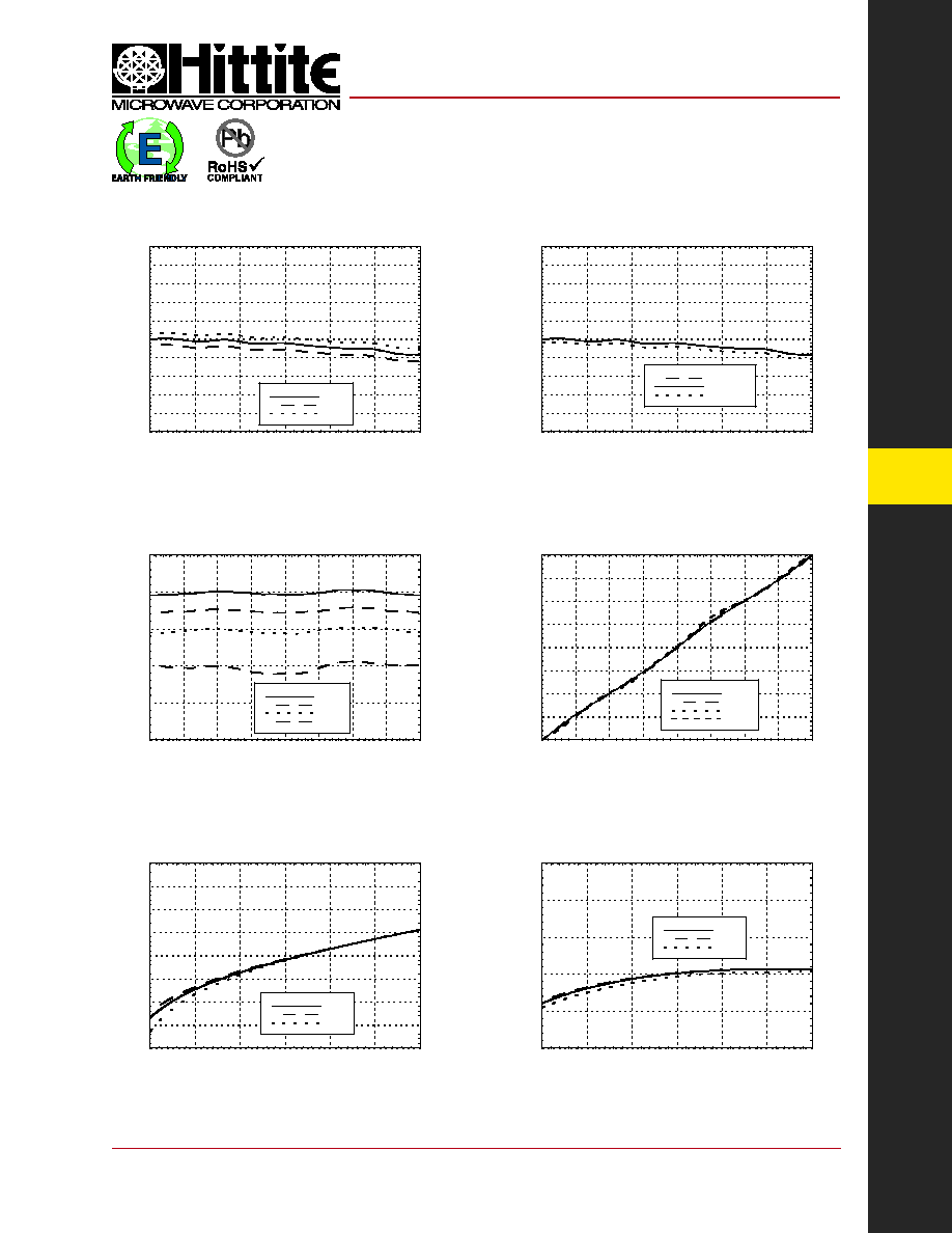
Input Return Loss vs. Temperature
Maximum Gain vs. Temperature
Maximum Gain vs. Supply Voltage
Gain vs. Phase Settings @ F= 2 GHz
Phase vs. Phase Settings @ F= 2 GHz
vs. Various Gain Settings
Output Return Loss vs. Temperature
-20
-18
-16
-14
-12
-10
-8
-6
-4
-2
0
1.7
1.8
1.9
2
2.1
2.2
2.3
+25C
+85C
-40C
GAIN
(dB)
FREQUENCY (GHz)
-20
-18
-16
-14
-12
-10
-8
-6
-4
-2
0
1.7
1.8
1.9
2
2.1
2.2
2.3
Vcc= 7.6V
Vcc= 8.0V
Vcc= 8.4V
GAIN
(dB)
FREQUENCY (GHz)
-50
-40
-30
-20
-10
0
0
45
90
135
180
225
270
315
360
Max.
-5dB
-10dB
-20dB
GAIN
(dB)
PHASE SETTING (DEGREES)
0
45
90
135
180
225
270
315
360
0
45
90
135
180
225
270
315
360
Max.
-5 dB
-10 dB
-20 dB
PHASE (DEGREES)
PHASE SETTING (DEGREES)
-40
-35
-30
-25
-20
-15
-10
-5
0
1.7
1.8
1.9
2
2.1
2.2
2.3
+25C
+85C
-40C
INPUT RETURN LOSS (dB)
FREQUENCY (GHz)
-25
-20
-15
-10
-5
0
1.7
1.8
1.9
2
2.1
2.2
2.3
+25C
+85C
-40C
OUTPUT RETURN LOSS (dB)
FREQUENCY (GHz)
GaAs HBT VECTOR
MODULATOR 1.8 - 2.2 GHz
v01.0705
HMC500LP3
/
500LP3E
13
MOD
U
L
A
T
O
R
S
- SM
T
13 - 36
For price, delivery, and to place orders, please contact Hittite Microwave Corporation:
20 Alpha Road, Chelmsford, MA 01824 Phone: 978-250-3343 Fax: 978-250-3373
Order On-line at www.hittite.com
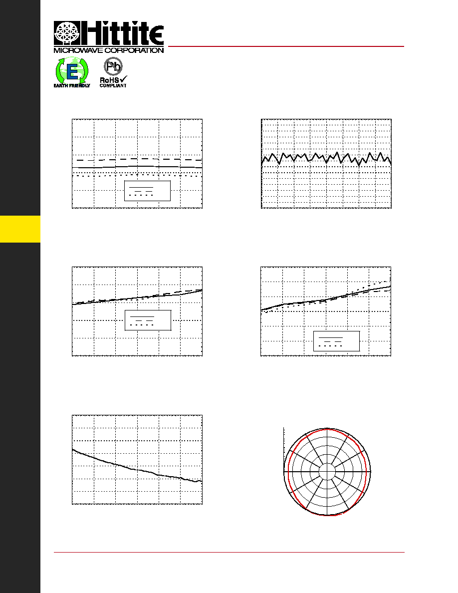
Input IP3 vs. Temperature
Output Noise vs. Temperature
Output Noise vs.
Phase Settings @ F= 2 GHz
Input P1dB vs. Temperature
Group Delay
-170
-168
-166
-164
-162
-160
1.7
1.8
1.9
2
2.1
2.2
2.3
+25 C
+85 C
-40 C
OUTPUT NOISE (dBm/Hz)
FREQUENCY (GHz)
-180
-178
-176
-174
-172
-170
-168
-166
-164
-162
-160
-158
-156
-154
-152
-150
0
45
90
135
180
225
270
315
360
OUTPUT NOISE (dBm/Hz)
PHASE SETTING (DEGREES)
10
12
14
16
18
20
1.7
1.8
1.9
2
2.1
2.2
2.3
+25 C
+85 C
-40 C
INPUT P1dB (dBm)
FREQUENCY (GHz)
26
28
30
32
34
36
38
1.7
1.8
1.9
2
2.1
2.2
2.3
+25 C
+85 C
-40 C
INPUT IP3 (dBm)
FREQUENCY (GHz)
620
640
660
680
700
720
740
760
1.7
1.8
1.9
2
2.1
2.2
2.3
GROUP DELAY (ps)
FREQUENCY (GHz)
Linear Gain vs. Phase Setting
0
0.2
0.4
0.6
0.8
1
0
30
60
90
120
210
240
270
300
330
MAGNITUDE G/Gmax
GaAs HBT VECTOR
MODULATOR 1.8 - 2.2 GHz
v01.0705
HMC500LP3
/
500LP3E
13
MOD
U
L
A
T
O
R
S
- SM
T
13 - 37
For price, delivery, and to place orders, please contact Hittite Microwave Corporation:
20 Alpha Road, Chelmsford, MA 01824 Phone: 978-250-3343 Fax: 978-250-3373
Order On-line at www.hittite.com
Absolute Maximum Ratings
RF Input (Vcc = +8V)
27 dBm
Supply Voltage (Vcc)
+10V
I & Q Input
-0.5V to +5.0V
Channel Temperature (Tc)
135 °C
Continuous Pdiss (T = 85°C)
(Derate 25 mW/°C above 85°C)
1.25 W
Thermal Resistance (R
th
)
(junction to ground paddle)
40 °C/W
Storage Temperature
-65 to +150 °C
Operating Temperature
-40 to +85 °C
Typical Supply Current vs. Vcc
Note:
Modulator will operate over full voltage range shown above.
Vcc (V)
Icc (mA)
7.6
85
8.0
90
8.4
95
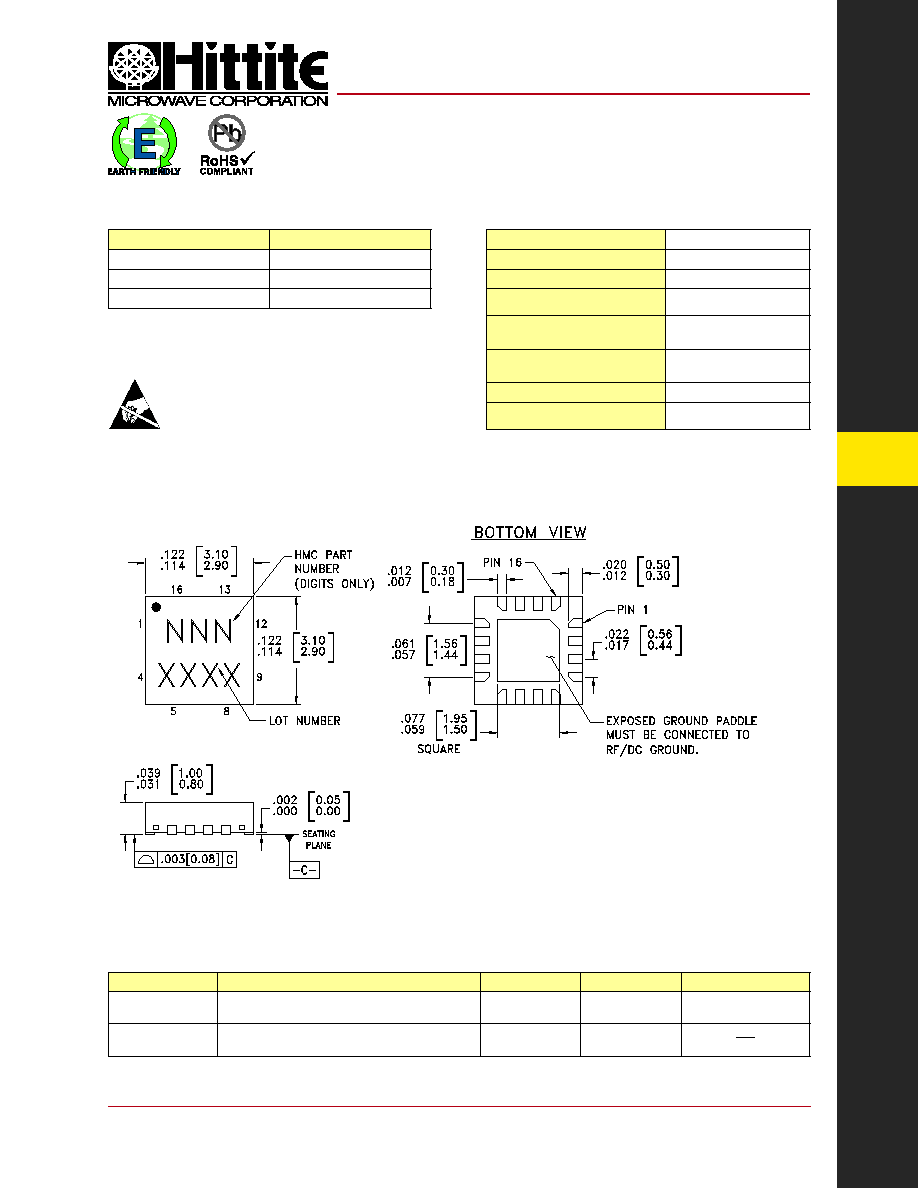
Outline Drawing
ELECTROSTATIC SENSITIVE DEVICE
OBSERVE HANDLING PRECAUTIONS
Part Number
Package Body Material
Lead Finish
MSL Rating
Package Marking
[3]
HMC500LP3
Low Stress Injection Molded Plastic
Sn/Pb Solder
MSL1
[1]
500
XXXX
HMC500LP3E
RoHS-compliant Low Stress Injection Molded Plastic
100% matte Sn
MSL1
[2]
500
XXXX
[1] Max peak refl ow temperature of 235 °C
[2] Max peak refl ow temperature of 260 °C
[3] 4-Digit lot number XXXX
Package Information
NOTES:
1. LEADFRAME MATERIAL: COPPER ALLOY
2. DIMENSIONS ARE IN INCHES [MILLIMETERS].
3. LEAD SPACING TOLERANCE IS NON-CUMULATIVE
4. PAD BURR LENGTH SHALL BE 0.15mm MAXIMUM.
PAD BURR HEIGHT SHALL BE 0.05mm MAXIMUM.
5. PACKAGE WARP SHALL NOT EXCEED 0.05mm.
6. ALL GROUND LEADS AND GROUND PADDLE MUST
BE SOLDERED TO PCB RF GROUND.
7. REFER TO HITTITE APPLICATION NOTE FOR SUGGESTED
PCB LAND PATTERN.
GaAs HBT VECTOR
MODULATOR 1.8 - 2.2 GHz
v01.0705
HMC500LP3
/
500LP3E
13
MOD
U
L
A
T
O
R
S
- SM
T
13 - 38
For price, delivery, and to place orders, please contact Hittite Microwave Corporation:
20 Alpha Road, Chelmsford, MA 01824 Phone: 978-250-3343 Fax: 978-250-3373
Order On-line at www.hittite.com
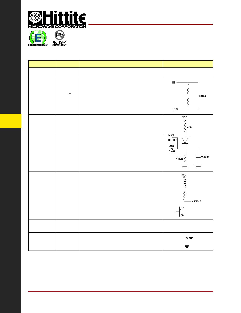
Pin Description
Pin Number
Function
Description
Interface Schematic
1, 4, 7, 8, 10 - 12,
N/C
No connection. These plus may be connected to RF ground.
Performance will not be affected
2, 3
IN, IN
Differential RF inputs, 50 Ohms. Must be DC blocked.
5, 15
I
In-phase control input. Pins 5 and 15 are redundant.
Either input can be used.
6, 16
Q
Quadrature control input. Pins 6 and 16 are redundant.
Either input can be used.
9
RFOUT
RF Output: Must be DC blocked.
13
Vcc
Supply Voltage
GND
Ground: Backside of package has exposed metal ground slug
which must be connected to RF/DC ground.
GaAs HBT VECTOR
MODULATOR 1.8 - 2.2 GHz
v01.0705
HMC500LP3
/
500LP3E