 | –≠–ª–µ–∫—Ç—Ä–æ–Ω–Ω—ã–π –∫–æ–º–ø–æ–Ω–µ–Ω—Ç: HMC538LP4 | –°–∫–∞—á–∞—Ç—å:  PDF PDF  ZIP ZIP |
14
S
W
I
T
C
H
E
S
- SM
T
14 - 288
For price, delivery, and to place orders, please contact Hittite Microwave Corporation:
20 Alpha Road, Chelmsford, MA 01824 Phone: 978-250-3343 Fax: 978-250-3373
Order On-line at www.hittite.com
HMC538LP4
/
538LP4E
600∞ ANALOG PHASE SHIFTER,
6 - 15 GHz
v00.0505
General Description
Features
Functional Diagram
The HMC538LP4 & HMC538LP4E are Analog Phase
Shifters which are controlled via an analog control volt-
age from 0 to +5V. THe HMC538LP4 & HMC538LP4E
provide a continuously variable phase shift of 0 to 800
degrees at 6 GHz, and 0 to 450 degrees at 16 GHz,
with consistent insertion loss versus phase shift. The
phase shift is monotonic with respect to control volt-
age. The control port has a modulation bandwidth
of 50 MHz. The low insertion loss and compact size
enable this part to be used in a wide range of applica-
tions, including the phase adjustment of clocks in fi ber
optic systems and test equipment. THe HMC538LP4
& HMC538LP4E are housed in leadless QFN surface
mount packages and are available in both standard
and RoHS compliant versions.
Available as Lead Free
Wide Bandwidth: 6 - 15 GHz
>600∞ Phase Shift
Single Positive Voltage Control
QFN Leadless SMT Package, 16 mm
2
Electrical Specifications,
T
A
= +25∞ C, 50 Ohm System
Typical Applications
The HMC538LP4 / HMC538LP4E is ideal for:
∑ Fiber Optics
∑ Military
∑ Test Equipment
Parameter
Frequency (GHz)
Min.
Typ.
Max.
Units
Phase Shift Range
6 - 10 GHz
10 - 15 GHz
600
360
800
600
degrees
degrees
Insertion Loss
6 - 15 GHz
8
11
dB
Return Loss (Input and Output)
6 - 15 GHz
7
dB
Control Voltage Range
6 - 15 GHz
0 - 5
Volt
Modulation Bandwidth
6 - 15 GHz
50
MHz
Phase Voltage Sensitivity
6 - 15 GHz
120
deg /Volt
Insertion Phase Temperature Sensitivity
6 - 15 GHz
0.5
deg /∞C

14
S
W
I
T
C
H
E
S
- SM
T
14 - 289
For price, delivery, and to place orders, please contact Hittite Microwave Corporation:
20 Alpha Road, Chelmsford, MA 01824 Phone: 978-250-3343 Fax: 978-250-3373
Order On-line at www.hittite.com
Phase Shift vs. Control Voltage
600∞ ANALOG PHASE SHIFTER,
6 - 15 GHz
v00.0505
HMC538LP4
/
538LP4E
Insertion Loss vs. Frequency
Phase Shift vs. Frequency @ Vctl = 5V
(Relative to Vctl = 0V)
Input Return Loss vs. Frequency,
Vctl = 0 to +5V
0
100
200
300
400
500
600
700
800
900
0
0.5
1
1.5
2
2.5
3
3.5
4
4.5
5
6GHz
11GHz
15GHz
NORMALIZED PHASE SHIFT (degrees)
Vctl (Vdc)
Output Return Loss vs. Frequency,
Vctl = 0 to +5V
-10
-9
-8
-7
-6
-5
-4
-3
-2
-1
0
0
0.5
1
1.5
2
2.5
3
3.5
4
4.5
5
+25C
+85C
-40C
INSERTION LOSS (dB)
Vctl (Vdc)
-20
-18
-16
-14
-12
-10
-8
-6
-4
-2
0
5
6
7
8
9
10
11
12
13
14
15
16
0V
1V
2V
3V
4V
5V
INSERTION LOSS (dB)
FREQUENCY (GHz)
-20
-15
-10
-5
0
5
6
7
8
9
10
11
12
13
14
15
16
RETURN LOSS (dB)
FREQUENCY (GHz)
-20
-15
-10
-5
0
5
6
7
8
9
10
11
12
13
14
15
16
RETURN LOSS (dB)
FREQUENCY (GHz)
0
100
200
300
400
500
600
700
800
900
5
6
7
8
9
10
11
12
13
14
15
16
+25C
+85C
-40C
NORMALIZED PHASE SHIFT (degrees)
FREQUENCY (GHz)
Insertion Loss vs. Control Voltage @ 11 GHz

14
S
W
I
T
C
H
E
S
- SM
T
14 - 290
For price, delivery, and to place orders, please contact Hittite Microwave Corporation:
20 Alpha Road, Chelmsford, MA 01824 Phone: 978-250-3343 Fax: 978-250-3373
Order On-line at www.hittite.com
Input IP3 vs. Control Voltage
Insertion Loss vs. Pin @ 11 GHz
Insertion Loss vs. Pin @ 7 GHz
Second Harmonics vs. Control Voltage,
Pin = -10 dBm
Insertion Loss vs. Pin @ 15 GHz
0
10
20
30
40
50
60
70
80
90
0
1
2
3
4
5
6 GHz
11 GHz
15 GHz
2nd HARMONICS (dBc)
Vctl (Vdc)
0
5
10
15
20
25
30
35
0
1
2
3
4
5
6 GHz
11 GHz
15 GHz
INPUT IP3 (dBm)
Vctl (Vdc)
-10
-9
-8
-7
-6
-5
-4
-3
-2
-1
0
-15
-10
-5
0
5
10
15
20
25
0V
2V
5V
INSERTION LOSS (dB)
INPUT POWER (dBm)
-10
-9
-8
-7
-6
-5
-4
-3
-2
-1
0
-15
-10
-5
0
5
10
15
20
25
0V
2V
5V
INSERTION LOSS (dB)
INPUT POWER (dBm)
-10
-9
-8
-7
-6
-5
-4
-3
-2
-1
0
-15
-10
-5
0
5
10
15
20
25
0V
2V
5V
INSERTION LOSS (dB)
INPUT POWER (dBm)
600∞ ANALOG PHASE SHIFTER,
6 - 15 GHz
v00.0505
Phase Shift vs. Pin @ 7 GHz
-10
-5
0
5
10
15
20
25
30
35
40
45
50
-20
-15
-10
-5
0
5
0v
2V
5V
NORMALIZED PHASE SHIFT (degrees)
INPUT POWER (dBm)
HMC538LP4
/
538LP4E

14
S
W
I
T
C
H
E
S
- SM
T
14 - 291
For price, delivery, and to place orders, please contact Hittite Microwave Corporation:
20 Alpha Road, Chelmsford, MA 01824 Phone: 978-250-3343 Fax: 978-250-3373
Order On-line at www.hittite.com
Absolute Maximum Ratings
Control Voltage (Vctl)
-1 Vdc to + 8 Vdc
Input Power (RFin)
+25 dBm
Channel Temperature (Tc)
150 ∞C
Continuous Pdiss (T = 85 ∞C)
(derate 21 mW/∞C above 85 ∞C)
1.36 W
Thermal Resistance
(junction to ground paddle)
48 ∞C/W
Storage Temperature
-65 to +150 ∞C
Operating Temperature
-40 to +85 ∞C
ESD Sensitivity (HBM)
Class 1B
Phase Shift vs. Pin @ 11 GHz
-5
0
5
10
15
20
-20
-15
-10
-5
0
5
0V
2V
5V
NORMALIZED PHASE SHIFT (degrees)
INPUT POWER (dBm)
Phase Shift vs. Pin @ 15 GHz
-10
-8
-6
-4
-2
0
2
4
6
8
10
-20
-15
-10
-5
0
5
0V
2V
5V
NORMALIZED PHASE SHIFT (degrees)
INPUT POWER (dBm)
600∞ ANALOG PHASE SHIFTER,
6 - 15 GHz
v00.0505
HMC538LP4
/
538LP4E

14
S
W
I
T
C
H
E
S
- SM
T
14 - 292
For price, delivery, and to place orders, please contact Hittite Microwave Corporation:
20 Alpha Road, Chelmsford, MA 01824 Phone: 978-250-3343 Fax: 978-250-3373
Order On-line at www.hittite.com
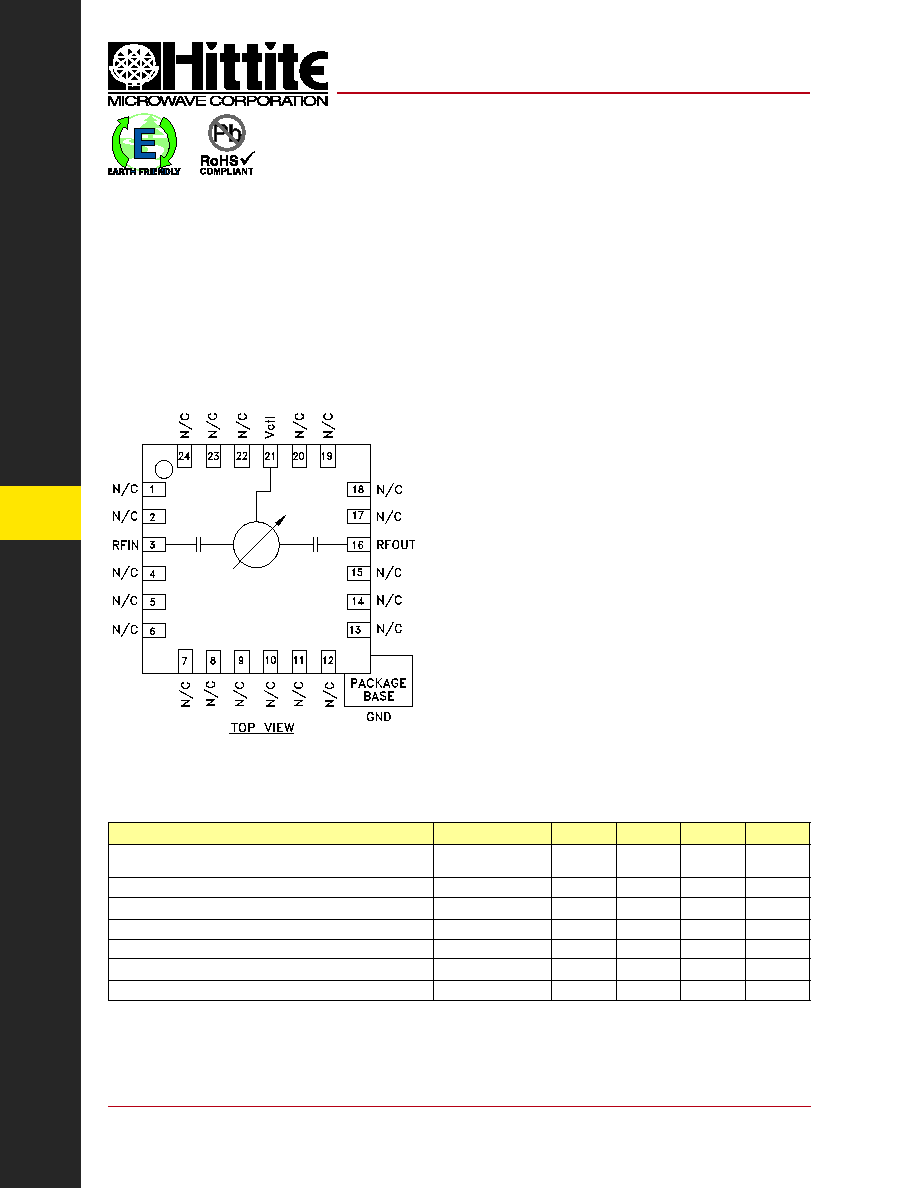
Pin Number
Function
Description
Interface Schematic
1, 2, 4-15,
17-20, 22-24
N/C
No connection required. These pins may be connected to
RF/DC ground without affecting performance.
3
RFIN
Port is DC blocked.
16
RFOUT
Port is DC blocked.
21
Vctl
Phase shift control pin. Application of a voltage between 0 and 5 volts causes
the transmission phase to change. The DC equivalent circuit is a series con-
nected diode and resistor.
GND
Ground: Backside of package has exposed metal ground slug that must be
connected to ground thru a short path. Vias under the device are required.
Pin Descriptions
Outline Drawing
600∞ ANALOG PHASE SHIFTER,
6 - 15 GHz
v00.0505
HMC538LP4
/
538LP4E
NOTES:
1. LEADFRAME MATERIAL: COPPER ALLOY
2. DIMENSIONS ARE IN INCHES [MILLIMETERS].
3. DIMENSION DOES NOT INCLUDE MOLDFLASH OF 0.15mm PER SIDE.
4. DIMENSION DOES NOT INCLUDE MOLDFLASH OF 0.25mm PER SIDE.
5. ALL GROUND LEADS MUST BE SOLDERED TO PCB RF GROUND.
6. CLASSIFIED AS MOISTURE SENSITIVITY LEVEL (MSL) 1.
Part Number
Package Body Material
Lead Finish
MSL Rating
Package Marking
[3]
HMC538LP4
Low Stress Injection Molded Plastic
Sn/Pb Solder
MSL1
[1]
H538
XXXX
HMC538LP4E
RoHS-compliant Low Stress Injection Molded Plastic
100% matte Sn
MSL1
[2]
H538
XXXX
[1] Max peak refl ow temperature of 235 ∞C
[2] Max peak refl ow temperature of 260 ∞C
[3] 4-Digit lot number XXXX
Package Information