A
T
T
E
N
U
A
T
O
R
S - SM
T
6
6 - 182
For price, delivery, and to place orders, please contact Hittite Microwave Corporation:
20 Alpha Road, Chelmsford, MA 01824 Phone: 978-250-3343 Fax: 978-250-3373
Order On-line at www.hittite.com
HMC542LP4
/
542LP4E
0.5 dB LSB GaAs MMIC 6-BIT DIGITAL
SERIAL CONTROL ATTENUATOR, DC - 3.0 GHz
v00.0306
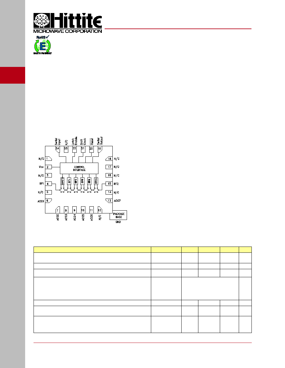
Functional Diagram
Electrical Specifications,
T
A
= +25∞ C, With Vcc = +5V
The HMC542LP4 / HMC542LP4E is ideal for both RF
and IF applications:
∑ Cellular/PCS/3G Infrastructure
∑ ISM, MMDS, WLAN, WiMAX, & WiBro
∑ Microwave Radio & VSAT
∑ Test Equipment and Sensors
0.5 dB LSB Steps to 31.5 dB
TTL/CMOS Compatible Serial Data Interface
SPI Compatible Serial Output
+/- 0.25 dB Typical Step Error
Single +5V Supply
4x4 mm SMT Package
The HMC542LP4 & HMC542LP4E are broadband
6-bit GaAs IC digital attenuators with CMOS com-
patible serial to parallel drivers in low cost lead-
less surface mount packages. This serial control
digital attenuator incorporates off chip AC ground
capacitors for near DC operation, making it suit-
able for a wide variety of RF and IF applications.
Covering DC to 3.0 GHz, the insertion loss is less
than 1.5 dB typical. The attenuator bit values are 0.5
(LSB), 1, 2, 4, 8, and 16 dB for a total attenuation of
31.5 dB. Attenuation accuracy is excellent at ± 0.25 dB
typical step error with an IIP3 of +45 dBm. Six bit serial
control words are used to select each attenuation
state. A single Vdd bias of +5V is required.
Parameter
Frequency (GHz)
Min.
Typ.
Max.
Units
Insertion Loss
DC - 1.5 GHz
1.5 - 3.0 GHz
1.2
1.5
1.5
1.8
dB
dB
Attenuation Range
DC - 3.0 GHz
31.5
dB
Return Loss (RF1 & RF2, All Atten. States)
DC - 3.0 GHz
17
dB
Attenuation Accuracy: (Referenced to Insertion Loss)
All Attenuation States
0.5 - 3.5 dB States
4.0 - 31.5 dB States
All Attenuation States
DC - 1.0 GHz
1.0 - 2.2 GHz
1.0 - 2.2 GHz
2.2 - 3.0 GHz
± (0.20 + 3% of Atten. Setting) Max.
± (0.25 + 3% of Atten. Setting) Max.
± (0.15 + 4% of Atten. Setting) Max.
± (0.30 + 3% of Atten. Setting) Max.
dB
dB
dB
dB
Input Power for 0.1 dB Compression
0.1 - 3.0 GHz
20
dBm
Input Third Order Intercept Point
(Two-Tone Input Power= 0 dBm Each Tone)
0.1 - 1.5 GHz
1.5 - 3.0 GHz
35
45
dBm
dBm
Switching Characteristics
tRISE, tFALL (10/90% RF)
tON, tOFF (50% CTL to 10/90% RF)
DC - 3.0 GHz
800
900
ns
ns
Typical Applications
Features
General Description

A
T
T
E
N
U
A
T
O
R
S - SM
T
6
6 - 183
For price, delivery, and to place orders, please contact Hittite Microwave Corporation:
20 Alpha Road, Chelmsford, MA 01824 Phone: 978-250-3343 Fax: 978-250-3373
Order On-line at www.hittite.com
Return Loss RF1, RF2
(Only Major States are Shown)
Insertion Loss
Normalized Attenuation
(Only Major States are Shown)
Bit Error vs. Frequency
(Only Major States are Shown)
Relative Phase vs. Frequency
(Only Major States are Shown)
Bit Error vs. Attenuation State
-3
-2.5
-2
-1.5
-1
-0.5
0
0
0.5
1
1.5
2
2.5
3
3.5
4
+25 C
+85 C
-40 C
INSERTION LOSS (dB)
FREQUENCY (GHz)
HMC542LP4
/
542LP4E
0.5 dB LSB GaAs MMIC 6-BIT DIGITAL
SERIAL CONTROL ATTENUATOR, DC - 3.0 GHz
v00.0306
-35
-30
-25
-20
-15
-10
-5
0
0
0.5
1
1.5
2
2.5
3
3.5
4
NORMALI
ZED ATTENUATI
ON (dB)
FREQUENCY (GHz)
-40
-20
0
20
40
60
80
0
0.5
1
1.5
2
2.5
3
3.5
4
RELATIVE PHASE (deg)
FREQUENCY (GHz)
8 dB
16 dB
31.5 dB
0.5-4 dB
-2
-1.5
-1
-0.5
0
0.5
1
1.5
2
0
0.5
1
1.5
2
2.5
3
3.5
4
BI
T ERROR (dB)
FREQUENCY (GHz)
16 dB
0.5-8B
31.5 dB
-40
-35
-30
-25
-20
-15
-10
-5
0
0
0.5
1
1.5
2
2.5
3
3.5
4
RETURN LOSS (dB)
FREQUENCY (GHz)
0.5-16 dB
31.5 dB
-1
-0.8
-0.6
-0.4
-0.2
0
0.2
0.4
0.6
0.8
1
0
4
8
12
16
20
24
28
32
BI
T ERROR (dB)
ATTENUATION STATE (dB)
3 GHz
2 GHz
1 GHz
500 MHz
40 MHz
100 MHz

A
T
T
E
N
U
A
T
O
R
S - SM
T
6
6 - 184
For price, delivery, and to place orders, please contact Hittite Microwave Corporation:
20 Alpha Road, Chelmsford, MA 01824 Phone: 978-250-3343 Fax: 978-250-3373
Order On-line at www.hittite.com
Worst Case Step Error
Between Successive Attenuation States
0.5 dB LSB GaAs MMIC 6-BIT DIGITAL
SERIAL CONTROL ATTENUATOR, DC - 3.0 GHz
v00.0306
-1
-0.8
-0.6
-0.4
-0.2
0
0.2
0.4
0.6
0.8
1
0
0.5
1
1.5
2
2.5
3
3.5
4
STEP ERROR (dB)
FREQUENCY (GHz)
HMC542LP4
/
542LP4E
Timing Diagram
Truth Table
Control Voltage Input
Attenua-
tion State
RF1 - RF2
C16
C8
C4
C2
C1
C0.5
High
High
High
High
High
High
Reference
I.L.
High
High
High
High
High
Low
0.5 dB
High
High
High
High
Low
High
1 dB
High
High
High
Low
High
High
2 dB
High
High
Low
High
High
High
4 dB
High
Low
High
High
High
High
8 dB
Low
High
High
High
High
High
16 dB
Low
Low
Low
Low
Low
Low
31.5 dB
Any combination of the above states will provide an attenuation
approximately equal to the sum of the bits selected.
CMOS Control Voltages
State
Vcc = +5V
Low
0 to 1.3V
High
3.5 to 5.0V
Parameter
Symbol
Vcc = +5V
Units
Min.
Max.
Serial Input Setup Time
ts
20
-
ns
Hold time from Serial
Input to Shift Clock
th
0
-
ns
Setup time from Shift
Clock to Latch Enable
tlsup
40
-
ns
Propagation delay, Latch
Enable to C0.5 through
C8
tpd
-
30
ns
Setup time from Reset to
Shift Clock
-
20
-
ns
Clock Frequency
(1/tclk)
fclk
-
30
MHz
Timing
Serial Input Truth Table
Latch
Enable
Shift
Clock
Reset
Function
X
X L
Shift
register
cleared
X
H
Shift register clocked
X
H
Contents of shift register
transferrred to Digital
Attenuator

A
T
T
E
N
U
A
T
O
R
S - SM
T
6
6 - 185
For price, delivery, and to place orders, please contact Hittite Microwave Corporation:
20 Alpha Road, Chelmsford, MA 01824 Phone: 978-250-3343 Fax: 978-250-3373
Order On-line at www.hittite.com
Logic / Functional Diagram
Programming Example to Select 16 dB Attenuation State
0.5 dB LSB GaAs MMIC 6-BIT DIGITAL
SERIAL CONTROL ATTENUATOR, DC - 3.0 GHz
v00.0306
HMC542LP4
/
542LP4E

A
T
T
E
N
U
A
T
O
R
S - SM
T
6
6 - 186
For price, delivery, and to place orders, please contact Hittite Microwave Corporation:
20 Alpha Road, Chelmsford, MA 01824 Phone: 978-250-3343 Fax: 978-250-3373
Order On-line at www.hittite.com
0.5 dB LSB GaAs MMIC 6-BIT DIGITAL
SERIAL CONTROL ATTENUATOR, DC - 3.0 GHz
v00.0306
HMC542LP4
/
542LP4E
Pin Number
Function
Description
Interface Schematic
1, 3, 5, 12, 14,
16-18, 23
N/C
These pins should be connected to PCB RF ground to
maximize performance.
2
Vcc
Supply Voltage.
4, 15
RF1, RF2
This pin is DC coupled and matched to 50 Ohms
Blocking capacitors are required. Select value based on
lowest frequency of operation.
6 - 11, 13
ACG1 - ACG7
External capacitor to ground is required. Select value for
lowest frequency of operation. Place capacitor as close to
pins as possible.
19
Serial Output
Serial data output. Serial input data
delayed by 8 clock cycles
20
Reset
See truth table, control voltage table and timing diagram.
21
Shift Clock
22
Latch Enable
24
Serial Input
GND
Package bottom has an exposed metal paddle
that must be connected to RF/DC Ground.
Pin Descriptions