3_mixer_chip_section.indd
M
I
X
E
R
S
- C
H
I
P
3
3 - 180
For price, delivery, and to place orders, please contact Hittite Microwave Corporation:
20 Alpha Road, Chelmsford, MA 01824 Phone: 978-250-3343 Fax: 978-250-3373
Order On-line at www.hittite.com
HMC554
GaAs MMIC FUNDAMENTAL
MIXER, 11 - 20 GHz
v00.1205
General Description
Features
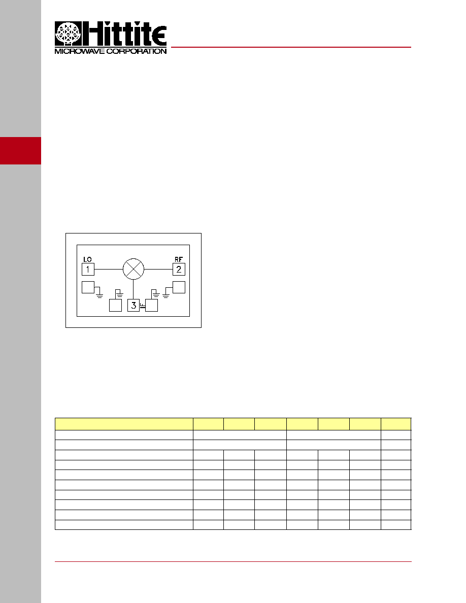
Functional Diagram
High LO to RF Isolation: 46 dB
Passive Double Balanced Topology
Low Conversion Loss: 7 dB
Wide IF Bandwidth: DC - 6 GHz
Small Size: 0.83 x 1.12 x 0.1 mm
Typical Applications
The HMC554 is ideal for:
� Microwave Radio
� VSAT
� Military & Space
� Communications, Radar & EW
The HMC554 is a passive double balanced mixer
that can be used as an upconverter or downconverter
between 11 and 20 GHz. The miniature monolithic
mixer is fabricated in a GaAs MESFET process, and
requires no external components or matching circu-
itry. The HMC554 provides excellent LO to RF and
LO to IF isolation due to optimized balun structures.
Measurements were made with the chip mounted
into in a 50 ohm test fi xture and includes the para-
sitic effects of wire bond assembly. Connections were
made with a 1 mil wire bond with minimal length (<12
mil).
Electrical Specifications,
T
A
= +25� C, IF= 100 MHz, LO= +13 dBm*
Parameter
Min.
Typ.
Max.
Min.
Typ.
Max.
Units
Frequency Range, RF & LO
12 - 16
11 - 20
GHz
Frequency Range, IF
DC - 6
DC - 6
GHz
Conversion Loss
7
9
8
10
dB
Noise Figure (SSB)
7
9
8
10
dB
LO to RF Isolation
40
46
38
44
dB
LO to IF Isolation
32
38
30
40
dB
RF to IF Isolation
16
25
15
25
dB
IP3 (Input)
18
18
dBm
IP2 (Input)
48
45
dBm
1 dB Gain Compression (Input)
11
11
dBm
*Unless otherwise noted, all measurements performed as downconverter, IF= 100 MHz.
M
I
X
E
R
S
- C
H
I
P
3
3 - 181
For price, delivery, and to place orders, please contact Hittite Microwave Corporation:
20 Alpha Road, Chelmsford, MA 01824 Phone: 978-250-3343 Fax: 978-250-3373
Order On-line at www.hittite.com
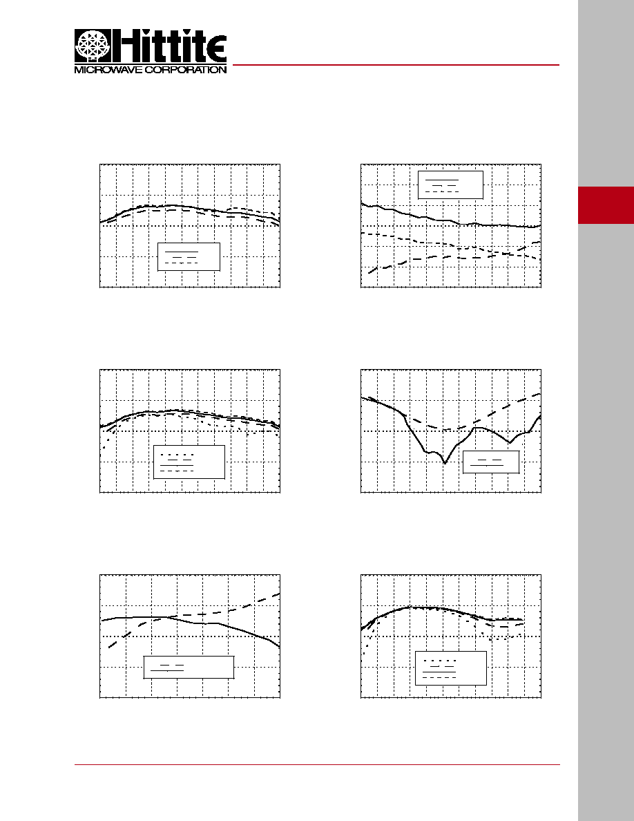
Conversion Gain vs.
Temperature @ LO = +13 dBm
Conversion Gain vs. LO Drive
Isolation @ LO = +13 dBm
IF Bandwidth @ LO = +13 dBm
Return Loss @ LO = +13 dBm
Upconverter Performance
Conversion Gain vs. LO Drive
-20
-15
-10
-5
0
10
11
12
13
14
15
16
17
18
19
20
21
+25C
+85C
-55C
CONVERSION GAIN (dB)
FREQUENCY (GHz)
HMC554
GaAs MMIC FUNDAMENTAL
MIXER, 11 - 20 GHz
v00.1205
-20
-15
-10
-5
0
10
11
12
13
14
15
16
17
18
19
20
21
LO
RF
RETURN LOSS (dB)
FREQUENCY (GHz)
-20
-15
-10
-5
0
10
11
12
13
14
15
16
17
18
19
20
21
+9 dBm
+11 dBm
+13 dBm
+15 dBm
CONVERSION GAIN (dB)
FREQUENCY (GHz)
-20
-15
-10
-5
0
10
11
12
13
14
15
16
17
18
19
20
21
+9 dBm
+11 dBm
+13 dBm
+15 dBm
CONVERSION GAIN (dB)
FREQUENCY (GHz)
-20
-15
-10
-5
0
0
1
2
3
4
5
6
7
IF Return Loss
Conversion Gain
RESPONSE (dB)
FREQUENCY (GHz)
-60
-50
-40
-30
-20
-10
0
10
11
12
13
14
15
16
17
18
19
20
21
RF/IF
LO/RF
LO/IF
ISOLATION (dB)
FREQUENCY (GHz)
M
I
X
E
R
S
- C
H
I
P
3
3 - 182
For price, delivery, and to place orders, please contact Hittite Microwave Corporation:
20 Alpha Road, Chelmsford, MA 01824 Phone: 978-250-3343 Fax: 978-250-3373
Order On-line at www.hittite.com
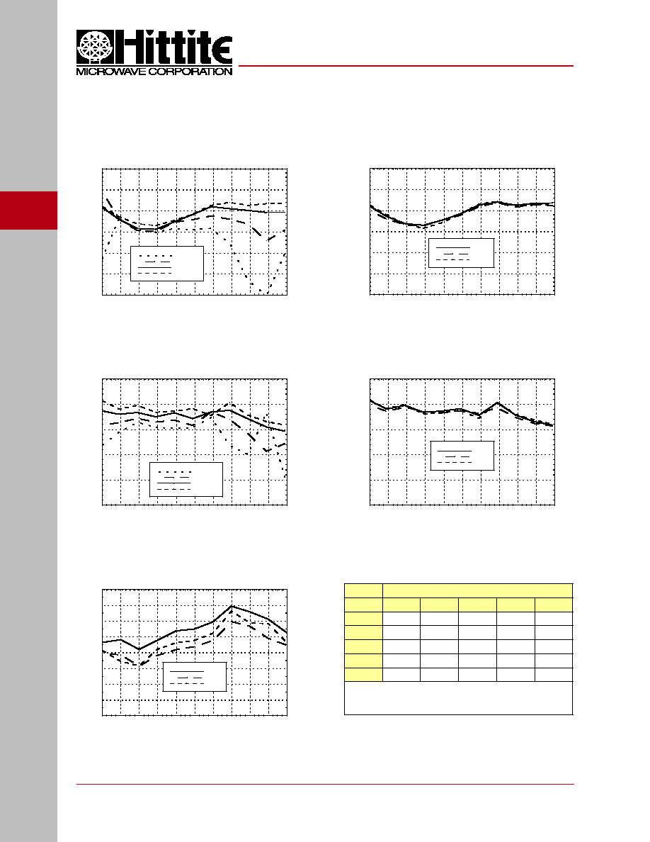
Input IP2 vs.
Temperature @ LO = +13 dBm *
Input IP3 vs. LO Drive *
Input IP3 vs.
Temperature @ LO = +13 dBm *
Input IP2 vs. LO Drive *
* Two-tone input power = -5 dBm each tone, 1 MHz spacing.
Input P1dB vs.
Temperature @ LO = +13 dBm
v00.1205
0
5
10
15
20
25
30
10
11
12
13
14
15
16
17
18
19
20
+9 dBm
+11 dBm
+13 dBm
+15 dBm
INPUT IP3 (dBm)
FREQUENCY (GHz)
HMC554
GaAs MMIC FUNDAMENTAL
MIXER, 11 - 20 GHz
10
20
30
40
50
60
10
11
12
13
14
15
16
17
18
19
20
+25C
+85C
-40C
INPUT IP2 (dBm)
FREQUENCY (GHz)
10
20
30
40
50
60
10
11
12
13
14
15
16
17
18
19
20
+9 dBm
+11 dBm
+13 dBm
+15 dBm
INPUT IP2 (dBm)
FREQUENCY (GHz)
0
5
10
15
20
25
30
10
11
12
13
14
15
16
17
18
19
20
+25 C
+85 C
-40 C
INPUT IP3 (dBm)
FREQUENCY (GHz)
MxN Spurious Outputs
nLO
mRF
0
1
2
3
4
0
xx
19
25
xx
xx
1
29
0
51
55
xx
2
81
85
60
88
104
3
xx
97
98
76
99
4
xx
xx
105
98
105
RF = 15.1 GHz @ -10 dBm
LO = 15.0 GHz @ +13 dBm
All values in dBc below the IF output power level.
6
7
8
9
10
11
12
13
14
10
11
12
13
14
15
16
17
18
19
20
+25C
+85C
-40C
INPUT P1dB (dBm)
FREQUENCY (GHz)
M
I
X
E
R
S
- C
H
I
P
3
3 - 183
For price, delivery, and to place orders, please contact Hittite Microwave Corporation:
20 Alpha Road, Chelmsford, MA 01824 Phone: 978-250-3343 Fax: 978-250-3373
Order On-line at www.hittite.com
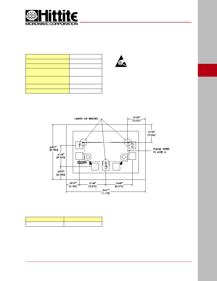
Outline Drawing
Absolute Maximum Ratings
NOTES:
1. ALL DIMENSIONS ARE IN INCHES [MM].
2. DIE THICKNESS IS .004".
3. TYPICAL BOND PAD IS .004" SQUARE.
4. BOND PAD SPACING CENTER TO CENTER IS .006".
5. BACKSIDE METALLIZATION: GOLD.
6. BOND PAD METALLIZATION: GOLD.
7. BACKSIDE METAL IS GROUND.
8. CONNECTION NOT REQUIRED FOR UNLABELED BOND PADS.
9. THIS DIE IS DESIGNED FOR PICK-UP WITH VACUUM (EDGE)
COLLET TOOLS. TO PRECLUDE THE RISK OF PERMANENT
DAMAGE, NO CONTACT TO THE DIE SURFACE IS ALLOWED
WITHIN THIS RECTANGULAR AREA.
Die Packaging Information
[1]
Standard
Alternate
WP-7
[2]
[1] Refer to the "Packaging Information" section for die
packaging dimensions.
[2] For alternate packaging information contact Hittite
Microwave Corporation.
ELECTROSTATIC SENSITIVE DEVICE
OBSERVE HANDLING PRECAUTIONS
v00.1205
RF / IF Input
+25 dBm
LO Drive
+25 dBm
Channel Temperature
150 �C
Continuous Pdiss (T = 85 �C)
(derate 3.26 mW/�C above 85 �C)
212 mW
Thermal Resistance
(channel to die bottom)
306 �C/W
Storage Temperature
-65 to +150 �C
Operating Temperature
-55 to +85 �C
HMC554
GaAs MMIC FUNDAMENTAL
MIXER, 11 - 20 GHz
M
I
X
E
R
S
- C
H
I
P
3
3 - 184
For price, delivery, and to place orders, please contact Hittite Microwave Corporation:
20 Alpha Road, Chelmsford, MA 01824 Phone: 978-250-3343 Fax: 978-250-3373
Order On-line at www.hittite.com
v00.1205
HMC554
GaAs MMIC FUNDAMENTAL
MIXER, 11 - 20 GHz
Pad Number
Function
Description
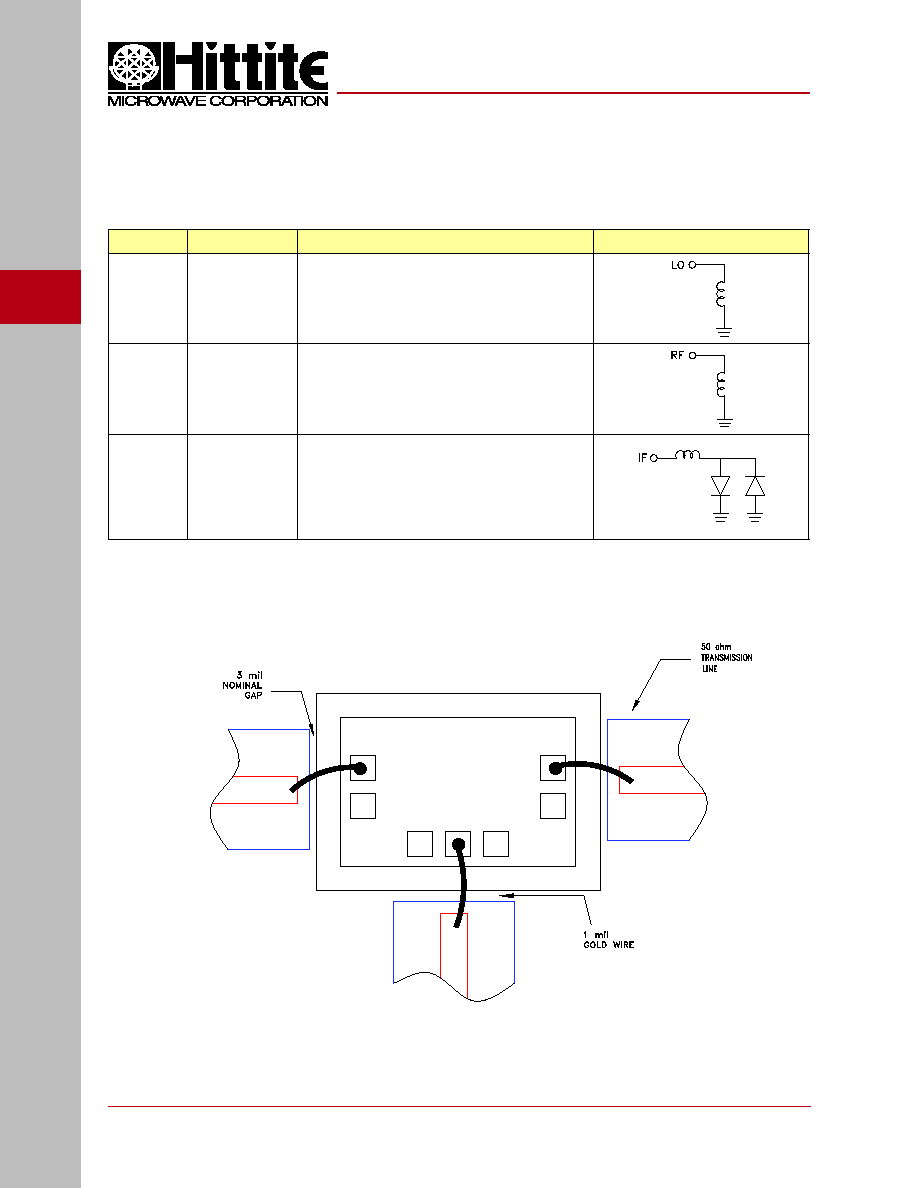
Interface Schematic
1
LO
This pad is DC coupled and matched
to 50 Ohm from 11 to 20 GHz.
2
RF
This pad is DC coupled and matched
to 50 Ohm from 11 to 20 GHz.
3
IF
This pad is DC coupled. For applications not requiring oper-
ation to DC, this port should be DC blocked externally using
a series capacitor whose value has been chosen to pass the
necessary IF frequency range. For operation to DC, this pin
must not source or sink more than 2 mA of current or part
non-function and possible part failure will result.
Pad Descriptions
Assembly Drawing