 | –≠–ª–µ–∫—Ç—Ä–æ–Ω–Ω—ã–π –∫–æ–º–ø–æ–Ω–µ–Ω—Ç: 7130A-1 | –°–∫–∞—á–∞—Ç—å:  PDF PDF  ZIP ZIP |
Document Outline
- ˛ˇ
- ˛ˇ
- ˛ˇ
- ˛ˇ
- ˛ˇ
- ˛ˇ
- ˛ˇ
- ˛ˇ
- ˛ˇ
- ˛ˇ
- ˛ˇ
- ˛ˇ
- ˛ˇ

HT71XX-1
30mA Voltage Regulator
Selection Table
Part No.
Output Voltage
Tolerance
Package
Marking
HT7130-1
3.0V
±3%
TO-92
SOT-89
SOT-25
71XXA-1 (for TO-92)
71XX-1 (for SOT-89)
1XX1 (for SOT-25)
HT7133-1
3.3V
±3%
HT7136-1
3.6V
±3%
HT7144-1
4.4V
±3%
HT7150-1
5.0V
±3%
Note:
≤XX≤ stands for output voltages.
Block Diagram
Rev. 1.10
1
August 22, 2002
Features
∑
Low power consumption
∑
Low voltage drop
∑
Low temperature coefficient
∑
High input voltage (up to 24V)
∑
Output voltage accuracy: tolerance
±3%
∑
TO-92, SOT-89 and SOT-25 package
Applications
∑
Battery-powered equipment
∑
Communication equipment
∑
Audio/Video equipment
General Description
The HT71XX-1 series is a set of three-terminal low
power high voltage regulators implemented in CMOS
technology. They allow input voltages as high as 24V.
They are available with several fixed output voltages
ranging from 3.0V to 5.0V. CMOS technology ensures
low voltage drop and low quiescent current.
Although designed primarily as fixed voltage regulators,
these devices can be used with external components to
obtain variable voltages and currents.
VOUT
VIN
GND
Vref

Pin Assignment
Pad Assignment
Pad Coordinates
Unit:
mm
Pad No.
X
Y
1
-429.00
-401.00
2
123.50
-401.00
3
416.00
-401.00
Chip size: 1111
¥1051 (mm)
2
* The IC substrate should be connected to VDD in the PCB layout artwork.
Absolute Maximum Ratings
Supply Voltage .........................................
-0.3V to 26V
Storage Temperature ...........................
-50∞C to 125∞C
Power Consumption (*1) .................................. 200mW
Operating Temperature ..............................0
∞C to 70∞C
Power Consumption (*2) ...................................150mW
Note: These are stress ratings only. Stresses exceeding the range specified under
≤Absolute Maximum Ratings≤ may
cause substantial damage to the device. Functional operation of this device at other conditions beyond those
listed in the specification is not implied and prolonged exposure to extreme conditions may affect device reliabil-
ity.
*1: applied to SOT-89 and TO-92
*2: applied to SOT-25
HT71XX-1
Rev. 1.10
2
August 22, 2002
T O - 9 2
G N D
V I N
V O U T
S O T - 8 9
V O U T
G N D V I N
7 1 X X A - 1
. r o n t V i e w
B o t t o m V i e w
S O T - 2 5
G N D
V I N
V O U T
G N D
V I N
V O U T
7 1 X X - 1
1 X X 1
N C
N C
T o p V i e w
G N D
V I N
V O U T
1
2
3
( 0 , 0 )
V
O
U
T
V
D
D
V
S
S
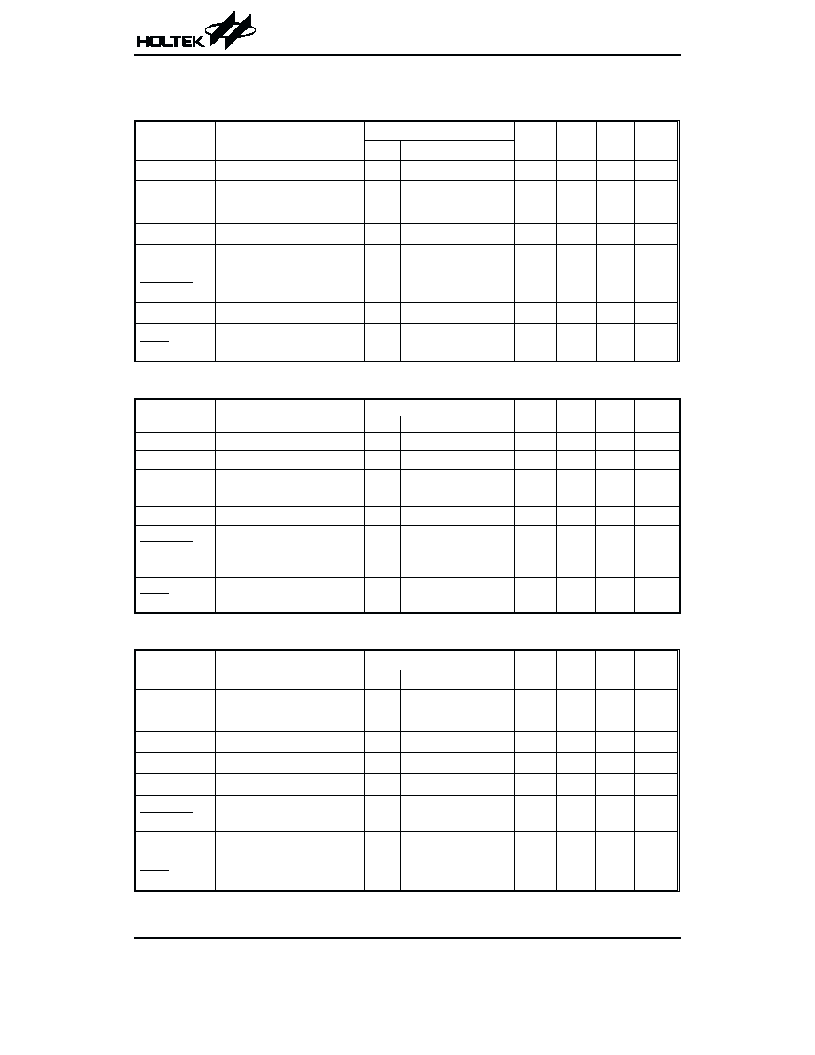
Electrical Characteristics
HT7130-1, +3.0V output type
Ta=25
∞C
Symbol
Parameter
Test Conditions
Min.
Typ.
Max.
Unit
V
IN
Conditions
V
OUT
Output Voltage
5V
I
OUT
=10mA
2.91
3
3.09
V
I
OUT
Output Current
5V
æ
20
30
æ
mA
DV
OUT
Load Regulation
5V
1mA
£I
OUT
£20mA
æ
60
100
mV
V
DIF
Voltage Drop
æ
I
OUT
=1mA
æ
100
æ
mV
I
SS
Current Consumption
5V
No load
æ
3
6
mA
D
D
V
V
V
OUT
IN
OUT
¥
Line Regulation
æ
4V
£V
IN
£24V
I
OUT
=1mA
æ
0.2
æ
%/V
V
IN
Input Voltage
æ
æ
æ
æ
24
V
D
D
V
T
OUT
a
Temperature Coefficient
5V
I
OUT
=10mA
0
∞C<Ta<70∞C
æ
±0.45
æ
mV/
∞C
HT7133-1, +3.3V output type
Ta=25
∞C
Symbol
Parameter
Test Conditions
Min.
Typ.
Max.
Unit
V
IN
Conditions
V
OUT
Output Voltage
5.5V
I
OUT
=10mA
3.201
3.3
3.399
V
I
OUT
Output Current
5.5V
æ
20
30
æ
mA
DV
OUT
Load Regulation
5.5V
1mA
£I
OUT
£30mA
æ
60
100
mV
V
DIF
Voltage Drop
æ
I
OUT
=1mA
æ
100
æ
mV
I
SS
Current Consumption
5.5V
No load
æ
3
6
mA
D
D
V
V
V
OUT
IN
OUT
¥
Line Regulation
æ
4.5V
£V
IN
£24V
I
OUT
=1mA
æ
0.2
æ
%/V
V
IN
Input Voltage
æ
æ
æ
æ
24
V
D
D
V
T
OUT
a
Temperature Coefficient
5.5V
I
OUT
=10mA
0
∞C<Ta<70∞C
æ
±0.5
æ
mV/
∞C
HT7136-1, +3.6V output type
Ta=25
∞C
Symbol
Parameter
Test Conditions
Min.
Typ.
Max.
Unit
V
IN
Conditions
V
OUT
Output Voltage
5.6V
I
OUT
=10mA
3.492
3.6
3.708
V
I
OUT
Output Current
5.6V
æ
20
30
æ
mA
DV
OUT
Load Regulation
5.6V
1mA
£I
OUT
£30mA
æ
60
100
mV
V
DIF
Voltage Drop
æ
I
OUT
=1mA
æ
60
æ
mV
I
SS
Current Consumption
5.6V
No load
æ
3
6
mA
D
D
V
V
V
OUT
IN
OUT
¥
Line Regulation
æ
4.6V
£V
IN
£24V
I
OUT
=1mA
æ
0.2
æ
%/V
V
IN
Input Voltage
æ
æ
æ
æ
24
V
D
D
V
T
OUT
a
Temperature Coefficient
5.6V
I
OUT
=10mA
0
∞C<Ta<70∞C
æ
±0.6
æ
mV/
∞C
HT71XX-1
Rev. 1.10
3
August 22, 2002

HT7144-1, +4.4V output type
Ta=25
∞C
Symbol
Parameter
Test Conditions
Min.
Typ.
Max.
Unit
V
IN
Conditions
V
OUT
Output Voltage
6.4V
I
OUT
=10mA
4.268
4.4
4.532
V
I
OUT
Output Current
6.4V
æ
20
30
æ
mA
DV
OUT
Load Regulation
6.4V
1mA
£I
OUT
£30mA
æ
60
100
mV
V
DIF
Voltage Drop
æ
I
OUT
=1mA
æ
100
æ
mV
I
SS
Current Consumption
6.4V
No load
æ
3
6
mA
D
D
V
V
V
OUT
IN
OUT
¥
Line Regulation
æ
5.4V
£V
IN
£24V
I
OUT
=1mA
æ
0.2
æ
%/V
V
IN
Input Voltage
æ
æ
æ
æ
24
V
D
D
V
T
OUT
a
Temperature Coefficient
6.4V
I
OUT
=10mA
0
∞C<Ta<70∞C
æ
±0.7
æ
mV/
∞C
HT7150-1, +5.0V output type
Ta=25
∞C
Symbol
Parameter
Test Conditions
Min.
Typ.
Max.
Unit
V
IN
Conditions
V
OUT
Output Voltage
7V
I
OUT
=10mA
4.85
5
5.15
V
I
OUT
Output Current
7V
æ
20
30
æ
mA
DV
OUT
Load Regulation
7V
1mA
£I
OUT
£30mA
æ
60
100
mV
V
DIF
Voltage Drop
æ
I
OUT
=1mA
æ
100
æ
mV
I
SS
Current Consumption
7V
No load
æ
3
6
mA
D
D
V
V
V
OUT
IN
OUT
¥
Line Regulation
æ
6V
£V
IN
£24V
I
OUT
=1mA
æ
0.2
æ
%/V
V
IN
Input Voltage
æ
æ
æ
æ
24
V
D
D
V
T
OUT
a
Temperature Coefficient
7V
I
OUT
=10mA
0
∞C<Ta<70∞C
æ
±0.75
æ
mV/
∞C
Application Circuits
Basic circuits
HT71XX-1
Rev. 1.10
4
August 22, 2002
H T 7 1 X X - 1
S e r i e s
C 1
1 0 m .
C o m m o n
C o m m o n
S i n g l e p o i n t G N D
G N D
V
I N
V
I N
V
O U T
V
O U T
C 2
1 0 m .
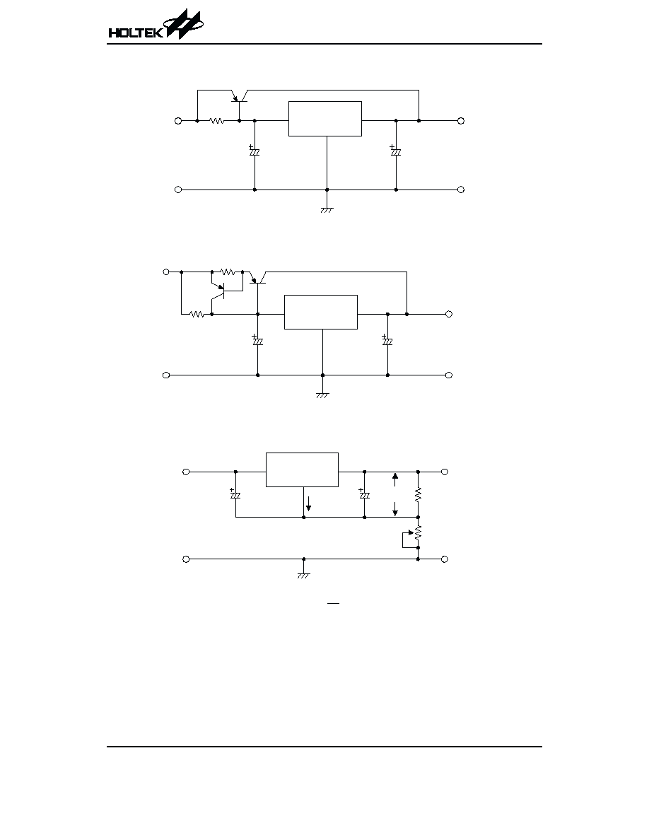
High output current positive voltage regulator
Short-Circuit protection by Tr1
Circuit for increasing output voltage
V
V
(1+
R2
R1
)
I
R2
OUT
XX
SS
=
+
HT71XX-1
Rev. 1.10
5
August 22, 2002
C o m m o n
C o m m o n
S i n g l e p o i n t G N D
G N D
T r 1
R 1
V
I N
V
I N
V
O U T
V
O U T
H T 7 1 X X - 1
S e r i e s
C 1
1 0 m .
C 2
1 0 m .
C o m m o n
C o m m o n
S i n g l e p o i n t G N D
G N D
T r 1
R s
R 1
V
I N
V
O U T
V
I N
V
O U T
H T 7 1 X X - 1
S e r i e s
C 1
1 0 m .
C 2
1 0 m .
C o m m o n
C o m m o n
S i n g l e p o i n t G N D
G N D
R 1
R 2
V
I N
V
O U T
V
I N
V
O U T
V
X X
I
S S
H T 7 1 X X - 1
S e r i e s
C 1
1 0 m .
C 2
1 0 m .