 | –≠–ª–µ–∫—Ç—Ä–æ–Ω–Ω—ã–π –∫–æ–º–ø–æ–Ω–µ–Ω—Ç: H49R50A-1 | –°–∫–∞—á–∞—Ç—å:  PDF PDF  ZIP ZIP |
Document Outline
- ˛ˇ
- ˛ˇ
- ˛ˇ
- ˛ˇ
- ˛ˇ
- ˛ˇ
- ˛ˇ
- ˛ˇ
- ˛ˇ
- ˛ˇ
- ˛ˇ
- ˛ˇ
- ˛ˇ
- ˛ˇ
- ˛ˇ

HT49R50A-1/HT49C50-1/HT49C50L
LCD Type 8-Bit MCU
Rev. 2.00
1
November 29, 2005
Features
∑
Operating voltage:
f
SYS
=4MHz: 2.2V~5.5V for HT49R50A-1/HT49C50-1
f
SYS
=8MHz: 3.3V~5.5V for HT49R50A-1/HT49C50-1
f
SYS
=500kHz: 1.2V~2.2V for HT49C50L
∑
8 input lines
∑
12 bidirectional I/O lines
∑
Two external interrupt input
∑
Two 8-bit programmable timer/event counter with
PFD (programmable frequency divider) function
∑
LCD driver with 33
¥2, 33¥3 or 32¥4 segments
∑
4K
¥15 program memory
∑
160
¥8 data memory RAM
∑
Real Time Clock (RTC)
∑
8-bit prescaler for RTC
∑
Watchdog Timer
∑
Buzzer output
∑
On-chip crystal, RC and 32768Hz crystal oscillator
∑
HALT function and wake-up feature reduce power
consumption
∑
6-level subroutine nesting
∑
Bit manipulation instruction
∑
15-bit table read instruction
∑
Up to 0.5
ms instruction cycle with 8MHz system clock
for HT49R50A-1/HT49C50-1
∑
Up to 8
ms instruction cycle with 500kHz system clock
for HT49C50L
∑
63 powerful instructions
∑
All instructions in 1 or 2 machine cycles
∑
Low voltage reset/detector function
for HT49R50A-1/HT49C50-1
∑
48-pin SSOP, 100-pin QFP package
General Description
The HT49R50A-1/HT49C50-1/HT49C50L are 8-bit,
high performance, RISC architecture microcontroller
devices specifically designed for a wide range of LCD
applications. The mask version HT49C50-1 and
HT49C50L are fully pin and functionally compatible with
the OTP version HT49R50A-1 device. The HT49C50L
is a low voltage version, with the ability to operate at a
minimum power supply of 1.2V, making it suitable for
single cell battery applications.
The advantages of low power consumption, I/O flexibil-
ity, programmable frequency divider, timer functions,
oscillator options, HALT and wake-up functions and
buzzer driver in addition to a flexible and configurable
LCD interface, enhance the versatility of these devices
to control a wide range of LCD-based application possi-
bilities such as measuring scales, electronic multi-
meters, gas meters, timers, calculators, remote
controllers and many other LCD-based industrial and
home appliance applications.
Technical Document
∑
Tools Information
∑
FAQs
∑
Application Note
-
HA0017E Controlling the Read/Write Function of the HT24 Series EEPROM Using the HT49 Series MCUs
-
HA0024E Using the RTC in the HT49 MCU Series
-
HA0025E Using the Time Base in the HT49 MCU Series
-
HA0026E Using the I/O Ports on the HT49 MCU Series
-
HA0027E Using the Timer/Event Counter in the HT49 MCU Series
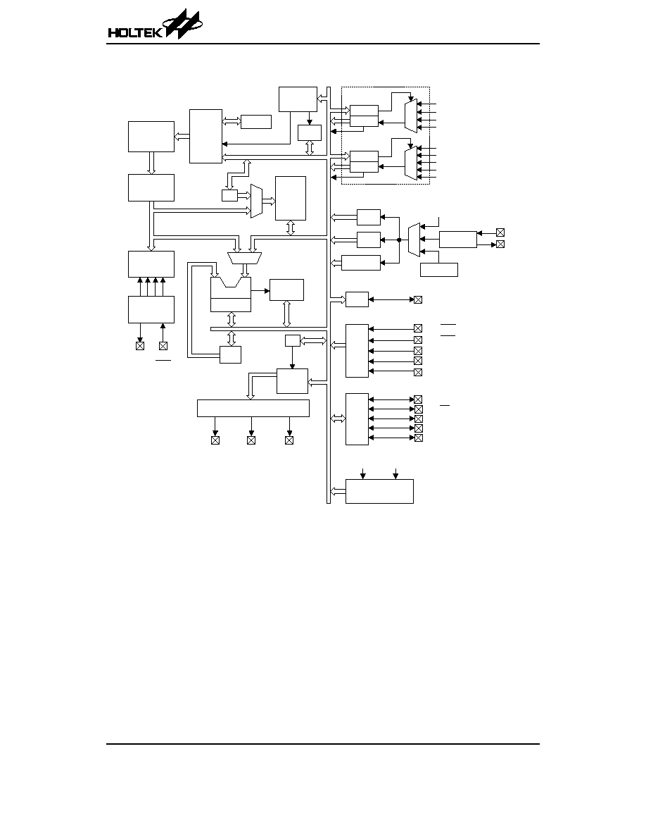
Block Diagram
HT49R50A-1/HT49C50-1/HT49C50L
Rev. 2.00
2
November 29, 2005
P r o g r a m
C o u n t e r
P r o g r a m
m e m o r y
I n s t r u c t i o n
R e g i s t e r
I n s t r u c t i o n
D e c o d e r
T i m i n g
G e n e r a t i o n
O S C 2
O S C 4
O S C 1
R E S
V D D
V S S
O S C 3
I n t e r r u p t
C i r c u i t
I N T C
M P
M
U
X
M U X
D A T A
M e m o r y
A L U
S h i f t e r
S T A T U S
A C C
P A
P O R T A
P A 0 / B Z
T M R 0 C
T M R 0
M
U
X
M
U
X
S Y S C L K / 4
P B
P O R T B
P B 2 / T M R 0
W D T O S C
P A 1 / B Z
P A 2
P A 3 / P F D
P A 4 ~ P A 7
P B 0 / I N T 0
P B 1 / I N T 1
P B 3 / T M R 1
R T C O S C
O S C 3
O S C 4
R T C
S T A C K
L C D
M e m o r y
B P
L C D D r i v e r
C O M 0 ~
C O M 2
C O M 3 /
S E G 3 2
S E G 0 ~
S E G 3 1
T i m e B a s e
W D T
P C
P C 0 ~ P C 3
P B 4 ~ P B 7
T M R 1 C
T M R 1
M
U
X
P F D 0
P F D 1
P B 3 / T M R 1
T M R 0 O V
f
S Y S
T i m e B a s e O u t
f
T 1 D
f
T 1 D
f
S Y S
R T C O u t
P B 2 / T M R 0
H A L T
E N / D I S
L V D / L V R
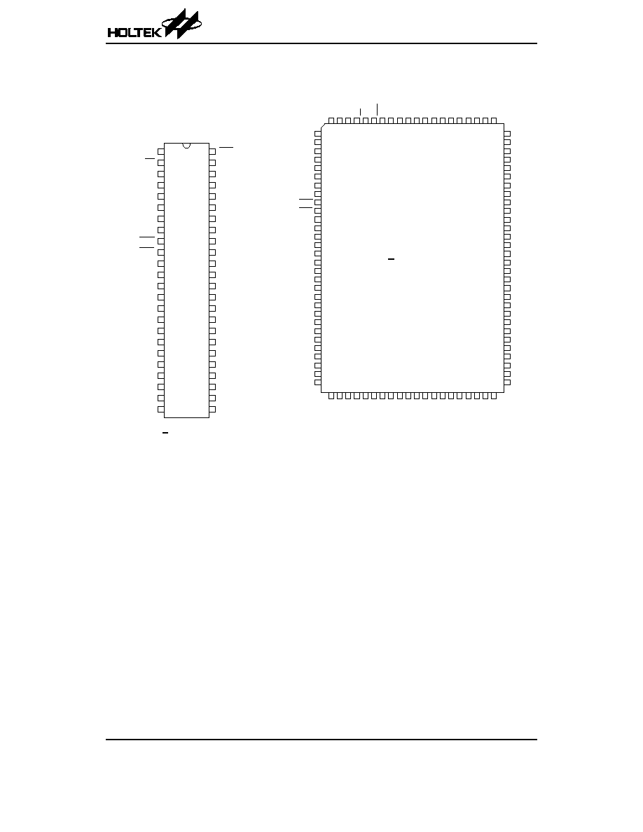
Pin Assignment
HT49R50A-1/HT49C50-1/HT49C50L
Rev. 2.00
3
November 29, 2005
4 8
4 7
4 6
4 5
4 4
4 3
4 2
4 1
4 0
3 9
3 8
3 7
3 6
3 5
3 4
3 3
3 2
3 1
3 0
2 9
2 8
2 7
2 6
2 5
1
2
3
4
5
6
7
8
9
1 0
1 1
1 2
1 3
1 4
1 5
1 6
1 7
1 8
1 9
2 0
2 1
2 2
2 3
2 4
P A 0 / B Z
P A 1 / B Z
P A 2
P A 3 / P F D
P A 4
P A 5
P A 6
P A 7
P B 0 / I N T 0
P B 1 / I N T 1
P B 2 / T M R 0
P B 3 / T M R 1
P B 4
P B 5
V S S
V L C D
V 1
V 2
C 1
C 2
C O M 0
C O M 1
C O M 2
C O M 3 / S E G 3 2
R E S
O S C 1
O S C 2
V D D
O S C 3
O S C 4
S E G 1 0
S E G 1 1
S E G 1 2
S E G 1 3
S E G 1 4
S E G 1 5
S E G 1 6
S E G 1 7
S E G 1 8
S E G 1 9
S E G 2 0
S E G 2 1
S E G 2 2
S E G 2 3
S E G 2 4
S E G 2 5
S E G 2 6
S E G 2 7
H T 4 9 R 5 0 A - 1 / H T 4 9 C 5 0 - 1 / H T 4 9 C 5 0 L
4 8 S S O P - A
H T 4 9 R 5 0 A - 1 / H T 4 9 C 5 0 - 1 / H T 4 9 C 5 0 L
1 0 0 Q F P - A
1
2
3
4
5
6
7
8
9
1 0
1 1
1 2
1 3
1 4
1 5
1 6
1 7
1 8
1 9
2 0
2 1
2 2
2 3
2 4
2 5
2 6
2 7
2 8
2 9
3 0
3 1 3 2 3 3 3 4 3 5 3 6 3 7 3 8 3 9 4 0 4 1 4 2 4 3 4 4 4 5 4 6 4 7 4 8 4 9 5 0
8 1
8 2
8 3
8 4
8 5
8 6
8 7
8 8
8 9
9 0
9 1
9 2
9 3
9 4
9 5
9 6
9 7
9 8
9 9
1 0 0
8 0
7 9
7 8
7 7
7 6
7 5
7 4
7 3
7 2
7 1
7 0
6 9
6 8
6 7
6 6
6 5
6 4
6 3
6 2
6 1
6 0
5 9
5 8
5 7
5 6
5 5
5 4
5 3
5 2
5 1
P A 5
N C
N C
N C
N C
N C
P A 6
P A 7
P B 0 / I N T 0
P B 1 / I N T 1
P B 2 / T M R 0
P B 3 / T M R 1
P B 4
P B 5
P B 6
P B 7
P C 0
P C 1
P C 2
P C 3
N C
N C
N C
N C
N C
N C
N C
N C
N C
V S S
N
C
S
E
G
2
2
S
E
G
2
3
S
E
G
2
4
S
E
G
2
5
S
E
G
2
6
S
E
G
2
7
S
E
G
2
8
S
E
G
2
9
S
E
G
3
0
S
E
G
3
1
C
O
M
3
/
S
E
G
3
2
C
O
M
2
C
O
M
1
C
O
M
0
C
2
C
1
V
2
V
1
V
L
C
D
S E G 1
S E G 2
S E G 3
N C
N C
N C
S E G 4
S E G 5
S E G 6
S E G 7
S E G 8
S E G 9
S E G 1 0
S E G 1 1
S E G 1 2
S E G 1 3
S E G 1 4
S E G 1 5
S E G 1 6
S E G 1 7
S E G 1 8
S E G 1 9
S E G 2 0
S E G 2 1
N C
N C
N C
N C
N C
N C
S
E
G
0
N
C
N
C
N
C
N
C
N
C
N
C
N
C
N
C
O
S
C
4
O
S
C
3
V
D
D
O
S
C
2
O
S
C
1
R
E
S
P
A
0
/
B
Z
P
A
1
/
B
Z
P
A
2
P
A
3
/
P
F
D
P
A
4
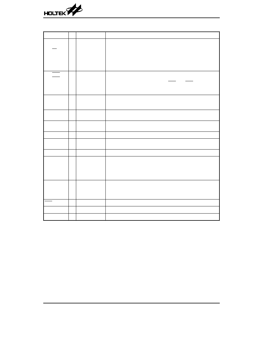
Pin Description
Pin Name
I/O
Options
Description
PA0/BZ
PA1/BZ
PA2
PA3/PFD
PA4~PA7
I/O
Wake-up
Pull-high or None
CMOS or NMOS
PA0~PA7 constitute an 8-bit bidirectional input/output port with Schmitt trig-
ger input capability. Each bit on port can be configured as wake-up input by
options. PA0~PA3 can be configured as CMOS output or NMOS input/out-
put with or without pull-high resistor by options. PA4~PA7 are always
pull-high NMOS input/output. Of the eight bits, PA0~PA1 can be set as I/O
pins or buzzer outputs by options. PA3 can be set as an I/O pin or as a PFD
output also by options.
PB0/INT0
PB1/INT1
PB2/TMR0
PB3/TMR1
PB4~PB7
I
æ
PB0~PB7 constitute an 8-bit Schmitt trigger input port. Each bit on port are
with pull-high resistor. Of the eight bits, PB0 and PB1 can be set as input
pins or as external interrupt control pins (INT0) and (INT1) respectively, by
software application. PB2 and PB3 can be set as input pin or as timer/event
counter input pin TMR0 and TMR1 also by software application.
PC0~PC3
I/O
Pull-high or None
CMOS or NMOS
PC0~PC3 constitute a 4-bit bidirectional input/output port with Schmitt trig-
ger input capability. On the port, such can be configured as CMOS output or
NMOS input/output with or without pull-high resistor by options.
V2
I
æ
Voltage pump for HT49R50A-1/HT49C50-1.
LCD power supply for HT49C50L.
VLCD
I
æ
LCD power supply for HT49R50A-1/HT49C50-1.
Voltage pump for HT49C50L.
V1, C1, C2
I
æ
Voltage pump
COM0~COM2
COM3/SEG32
O
1/2, 1/3 or 1/4
Duty
SEG32 can be set as a segment or as a common output driver for LCD
panel by options. COM0~COM2 are outputs for LCD panel plate.
SEG0~SEG31
O
æ
LCD driver outputs for LCD panel segments
OSC1
OSC2
I
O
Crystal or RC
OSC1 and OSC2 are connected to an RC network or a crystal (by options)
for the internal system clock. In the case of RC operation, OSC2 is the out-
put terminal for 1/4 system clock.
The system clock may come from the RTC oscillator. If the system clock co-
mes from RTCOSC, these two pins can be floating.
OSC3
OSC4
I
O
RTC or
System Clock
Real time clock oscillators. OSC3 and OSC4 are connected to a 32768Hz
crystal oscillator for timing purposes or to a system clock source (depend-
ing on the options).
No built-in capacitor
RES
I
æ
Schmitt trigger reset input, active low.
VSS
æ
æ
Negative power supply, ground
VDD
æ
æ
Positive power supply
Absolute Maximum Ratings
Supply Voltage..........................V
SS
-0.3V to V
SS
+6.0V*
Supply Voltage ........................V
SS
-0.3V to V
SS
+2.5V**
Storage Temperature ............................
-50∞C to 125∞C
Input Voltage..............................V
SS
-0.3V to V
DD
+0.3V
Operating Temperature ...........................
-40∞C to 85∞C
Note: These are stress ratings only. Stresses exceeding the range specified under
≤Absolute Maximum Ratings≤ may
cause substantial damage to the device. Functional operation of this device at other conditions beyond those
listed in the specification is not implied and prolonged exposure to extreme conditions may affect device reliabil-
ity.
≤*≤ For HT49R50A-1/HT49C50-1
≤**≤ For HT49C50L
HT49R50A-1/HT49C50-1/HT49C50L
Rev. 2.00
4
November 29, 2005
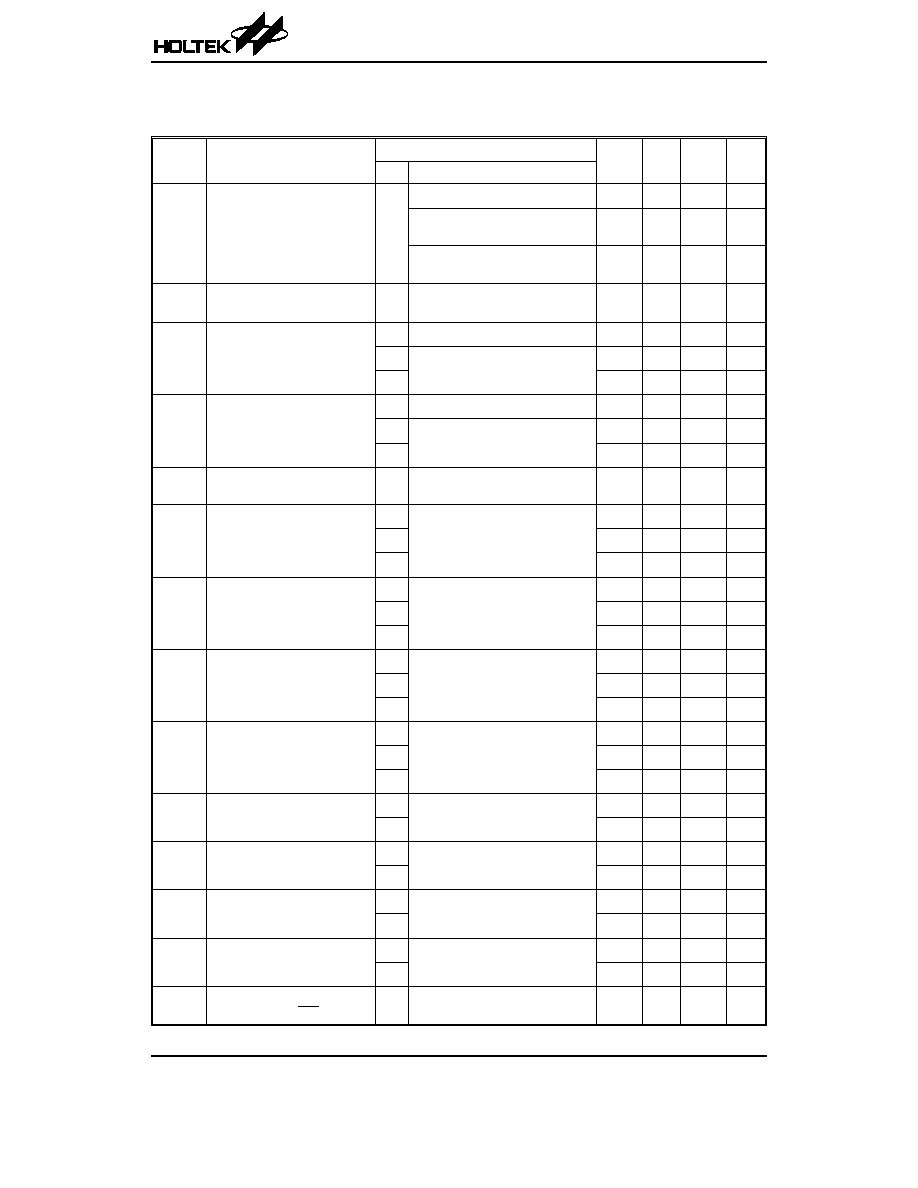
D.C. Characteristics
V
DD
=1.5V for HT49C50L, V
DD
=3V & V
DD
=5V for HT49R50A-1 and HT49C50-1
Ta=25
∞C
Symbol
Parameter
Test Conditions
Min.
Typ.
Max.
Unit
V
DD
Conditions
V
DD
Operating Voltage
æ
For HT49C50L
1.2
æ
2.2
V
LVR disable, f
SYS
=4MHz
(for HT49R50A-1/HT49C50-1)
2.2
æ
5.5
V
f
SYS
=8MHz
(for HT49R50A-1/HT49C50-1)
3.3
æ
5.5
V
V
LCD
LCD Power Supply (Note *)
æ
For HT49R50A-1/HT49C50-1,
VA
£5.5V
2.2
æ
5.5
V
I
DD1
Operating Current
(Crystal OSC)
1.5V No load, f
SYS
=455kHz
æ
60
100
mA
3V
No load, f
SYS
=4MHz
æ
1
2
mA
5V
æ
3
5
mA
I
DD2
Operating Current
(RC OSC)
1.5V No load, f
SYS
=400kHz
æ
50
100
mA
3V
No load, f
SYS
=4MHz
æ
1
2
mA
5V
æ
3
5
mA
I
DD3
Operating Current
(Crystal OSC, RC OSC)
5V
No load, f
SYS
=8MHz
æ
4
8
mA
I
DD4
Operating Current
(f
SYS
=RTC OSC)
1.5V
No load
æ
2.5
5
mA
3V
æ
0.3
0.6
mA
5V
æ
0.6
1
mA
I
STB1
Standby Current
(*f
S
=T1)
1.5V
No load, system HALT,
LCD off at HALT
æ
0.1
0.5
mA
3V
æ
æ
1
mA
5V
æ
æ
2
mA
I
STB2
Standby Current
(*f
S
=RTC OSC)
1.5V
No load, system HALT,
LCD On at HALT, C type
æ
1
2
mA
3V
æ
2.5
5
mA
5V
æ
10
20
mA
I
STB3
Standby Current
(*f
S
=WDT RC OSC)
1.5V
No load, system HALT
LCD On at HALT, C type
æ
0.5
1
mA
3V
æ
2
5
mA
5V
æ
6
10
mA
I
STB4
Standby Current
(*f
S
=RTC OSC)
3V
No load, system HALT,
LCD on at HALT, R type, 1/2 bias
æ
17
30
mA
5V
æ
34
60
mA
I
STB5
Standby Current
(*f
S
=RTC OSC)
3V
No load, system HALT,
LCD on at HALT, R type, 1/3 bias
æ
13
25
mA
5V
æ
26
50
mA
I
STB6
Standby Current
(*f
S
=WDT RC OSC)
3V
No load, system HALT,
LCD on at HALT, R type, 1/2 bias
æ
14
25
mA
5V
æ
28
50
mA
I
STB7
Standby Current
(*f
S
=WDT RC OSC)
3V
No load, system HALT,
LCD on at HALT, R type, 1/3 bias
æ
10
20
mA
5V
æ
20
40
mA
V
IL1
Input Low Voltage for I/O
Ports, TMR and INT
æ
æ
0
æ
0.3V
DD
V
HT49R50A-1/HT49C50-1/HT49C50L
Rev. 2.00
5
November 29, 2005