 | –≠–ª–µ–∫—Ç—Ä–æ–Ω–Ω—ã–π –∫–æ–º–ø–æ–Ω–µ–Ω—Ç: HA0005E | –°–∫–∞—á–∞—Ç—å:  PDF PDF  ZIP ZIP |
Document Outline
- ˛ˇ
- ˛ˇ
- ˛ˇ
- ˛ˇ
- ˛ˇ
- ˛ˇ
- ˛ˇ
- ˛ˇ
- ˛ˇ
- ˛ˇ
- ˛ˇ
- ˛ˇ
- ˛ˇ
- ˛ˇ
- ˛ˇ

HT46R14
A/D Type 8-Bit OTP MCU
Rev. 1.00
1
November 1, 2005
General Description
The device are 8-bit, high performance, RISC architec-
ture microcontroller devices specifically designed for
A/D applications that interface directly to analog signals,
such as those from sensors.
The advantages of low power consumption, I/O flexibil-
ity, programmable frequency divider, timer functions,
oscillator options, multi-channel A/D Converter, HALT
and wake-up functions, enhance the versatility of these
devices to suit a wide range of A/D application possibili-
ties such as sensor signal processing, etc.
The device provides two comparators and programma-
ble pulse generator (PPG). It is particularly suitable for
use in products such as induction cooker and home ap-
pliances.
Features
∑
Operating voltage:
f
SYS
=4MHz: 2.2V~5.5V
f
SYS
=8MHz: 3.3V~5.5V
∑
20 bidirectional I/O lines
∑
Two interrupt input shared with an I/O line
∑
Two 8-bit programmable timer/event counter with
overflow interrupt and 7-stage prescaler
∑
Two 8-bit programmable pulse generator (PPG) out-
put channels, with prescaler and 8-bit programmable
timer counter, and supports active low or active high
output
∑
On-chip crystal and RC oscillator
∑
Watchdog Timer
∑
4096
¥15 program memory
∑
192
¥8 data memory RAM
∑
Supports PFD for sound generation
∑
HALT function and wake-up feature reduce power
consumption
∑
Up to 0.5
ms instruction cycle with 8MHz system clock
at V
DD
=5V
∑
8-level subroutine nesting
∑
8 channels 9-bit resolution A/D converter
∑
Two comparators with interrupt function
∑
Bit manipulation instruction
∑
15-bit table read instruction
∑
63 powerful instructions
∑
All instructions in one or two machine cycles
∑
Low voltage reset function
∑
28-pin SKDIP/SOP package
Technical Document
∑
Tools Information
∑
FAQs
∑
Application Note
-
HA0004E HT48 & HT46 MCU UART Software Implementation Method
-
HA0005E Controlling the I2C bus with the HT48 & HT46 MCU Series
-
HA0011E HT48 & HT46 Keyboard Scan Program
-
HA0013E HT48 & HT46 LCM Interface Design
-
HA0102E Using the HT46R14 in a CCFL Lamp Inverter
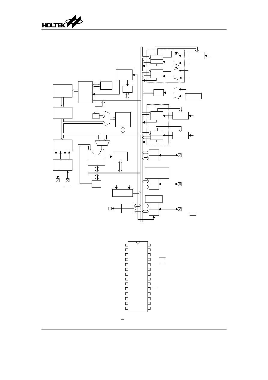
Block Diagram
Pin Assignment
HT46R14
Rev. 1.00
2
November 1, 2005
O S C 2
O S C 1
R E S
V D D
M U X
P A C
P A
P o r t A
P o r t B
V S S
P r o g r a m
R O M
P r o g r a m
C o u n t e r
I n t e r r u p t
C i r c u i t
S t a c k
I N T C
D a t a
M e m o r y
I n s t r u c t i o n
R e g i s t e r
M
U
X
I n s t r u c t i o n
D e c o d e r
S T A T U S
A L U
S h i f t e r
A C C
M P
L V R
P P G C
M
U
X
M
U
X
W D T O S C
W D T
M
U
X
P F D 0
P F D 1
f
S Y S
/ 4
f
S Y S
P r e s c a l e r
T M R 0
f
S Y S
/ 4
T M R 1
T M R 0 C
T M R 0
T M R 1 C
T M R 1
P P G 0
P P G 1
f
S Y S
P r e s c a l e r
P P G 0 C
P P G T 0
P P G 1 C
P P G T 1
f
S Y S
P r e s c a l e r
P o r t C
P C C
P C
8 - C h a n n e l
A / D C o n v e r t e r
P B C
P B
P A 0 / P P G 1
P A 1 ~ P A 2
P A 3 / P F D
P A 4 / T M R 0
P A 5 / I N T 0
P A 6 / I N T 1
P A 7 / T M R 1
P B 0 / A N 0 ~ P B 7 / A N 7
P P G 0 C
P P G 0
P P G 0
H A L T
E N / D I S
T i m i n g
G e n e r a t o r
P C 0 / C 0 V I N -
P C 1 / C 0 V I N +
P C 2 / C 0 O U T
P C 3 / C 1 O U T
H T 4 6 R 1 4
2 8 S K D I P - A / S O P - A
2 8
2 7
2 6
2 5
2 4
2 3
2 2
2 1
2 0
1 9
1 8
1 7
1 6
1 5
1
2
3
4
5
6
7
8
9
1 0
1 1
1 2
1 3
1 4
P B 1 / A N 1
P B 0 / A N 0
P A 3 / P F D
P A 2
P A 1
P A 0 / P P G 1
P B 7 / A N 7
P B 6 / A N 6
P B 5 / A N 5
P B 4 / A N 4
V S S
C 1 V I N +
C 1 V I N -
P C 3 / C 1 O U T
P B 2 / A N 2
P B 3 / A N 3
P A 4 / T M R 0
P A 5 / I N T 0
P A 6 / I N T 1
P A 7 / T M R 1
O S C 2
O S C 1
V D D
R E S
P P G 0
P C 0 / C 0 V I N -
P C 1 / C 0 V I N +
P C 2 / C 0 O U T

Pin Description
Pin Name
I/O
Option
Description
PA0/PPG1
PA1~PA2
PA3/PFD
PA4/TMR0
PA5/INT0
PA6/INT1
PA7/TMR1
I/O
Pull-high
Wake-up
PA3 or PFD
Bidirectional 8-bit input/output port. Each bit can be configured as wake-up in-
put by options. Software instructions determine the CMOS output or Schmitt
trigger input with or without pull-high resistor (determined by pull-high option:
bit option).
The PFD, INT0 and INT1 are pin-shared with PA3, PA5 and PA6. The TMR0
is pin-shared with PA4, TMR1 is pin shared with PA7, respectively.
The PPG1 is a programmable pulse generator1 output pin, pin shared with
PA0. The PPG1 or I/O function is selected via configuration option. The PPG1
output pin is floating during power-on reset, RES pin reset or LVR reset. The
PPG1 output level (active low or active high) can be selected via configuration
option.
PB0/AN0~
PB7/AN7
I/O
Pull-high
Bidirectional 8-bit input/output port. Software instructions determine the
CMOS output, Schmitt trigger input with or without pull-high resistor (deter-
mined by pull-high option: bit option) or A/D input.
Once a PB line is selected as an A/D input (by using software control), the I/O
function and pull-high resistor are disabled automatically.
PC0/C0VIN-
PC1/C0VIN+
PC2/C0OUT
PC3/C1OUT
C1VIN+
C1VIN-
I/O
Pull-high
I/O or
Comparator
Bidirectional 4-bit input/output port. Software instructions determine the
CMOS output, Schmitt trigger input with or without pull-high resistor (deter-
mine by pull-high option: byte option).
C0VIN+, C0VIN- and C0OUT are pin-shared with PC1, PC0 and PC2. Once
the Comparator 0 function is used, the internal registers related to PC1, PC0
cannot be used, PC2 can be used as input only, the PC1, PC0 I/O function,
PC2 output function and pull-high resistor are disabled automatically. Soft-
ware instructions determine the Comparator 0 function to be used.
C1VIN+ and C1VIN- are Comparator 1 input, C1OUT is pin-shared with PC3.
Once the Comparator 1 function is used, the internal register related to PC3
can be used as input only, the PC3 output function and pull-high resistor are
disabled automatically. Software instructions determine the Comparator 1
function to be used.
PPG0
O
æ
This is a programmable pulse generator 0 output pin, the pin is floating during
power-on reset, RES pin reset or LVR reset. The PPG0 output level (active
low or active high) can be selected via configuration option
OSC1
OSC2
I
O
Crystal
or RC
OSC1, OSC2 are connected to an RC network or a Crystal (determined by op-
tions) for the internal system clock. In the case of RC operation, OSC2 is the
output terminal for 1/4 system clock.
RES
I
æ
Schmitt trigger reset input. Active low.
VDD
æ
æ
Positive power supply
VSS
æ
æ
Negative power supply, ground
Absolute Maximum Ratings
Supply Voltage ...........................V
SS
-0.3V to V
SS
+6.0V
Storage Temperature ............................
-50∞C to 125∞C
Input Voltage..............................V
SS
-0.3V to V
DD
+0.3V
Operating Temperature...........................
-40∞C to 85∞C
Note: These are stress ratings only. Stresses exceeding the range specified under
≤Absolute Maximum Ratings≤ may
cause substantial damage to the device. Functional operation of this device at other conditions beyond those
listed in the specification is not implied and prolonged exposure to extreme conditions may affect device reliabil-
ity.
HT46R14
Rev. 1.00
3
November 1, 2005

D.C. Characteristics
Symbol
Parameter
Test Conditions
Min.
Typ.
Max.
Unit
V
DD
Conditions
V
DD
Operating Voltage
æ
f
SYS
=4MHz
2.2
æ
5.5
V
æ
f
SYS
=8MHz
3.3
æ
5.5
V
I
DD1
Operating Current (Crystal OSC)
3V
No load, f
SYS
=4MHz
ADC disable
æ
0.6
1.5
mA
5V
æ
2
4
mA
I
DD2
Operating Current (RC OSC)
3V
No load, f
SYS
=4MHz
ADC disable
æ
0.8
1.5
mA
5V
æ
2.5
4
mA
I
DD3
Operating Current
(Crystal OSC, RC OSC)
5V
No load, f
SYS
=8MHz
ADC disable
æ
4
8
mA
I
STB1
Standby Current (WDT Enabled)
3V
No load, system HALT
æ
æ
5
mA
5V
æ
æ
10
mA
I
STB2
Standby Current (WDT Disabled)
3V
No load, system HALT
æ
æ
1
mA
5V
æ
æ
2
mA
V
IL1
Input Low Voltage for I/O Ports,
TMR0 and TMR1
æ
æ
0
æ
0.3V
DD
V
V
IH1
Input High Voltage for I/O Ports,
TMR0 and TMR1
æ
æ
0.7V
DD
æ
V
DD
V
V
IL2
Input Low Voltage (RES)
æ
æ
0
æ
0.4V
DD
V
V
IH2
Input High Voltage (RES)
æ
æ
0.9V
DD
æ
V
DD
V
V
LVR
Low Voltage Reset
æ
æ
2.7
3
3.3
V
I
OL
I/O Port Sink Current
3V
V
OL
=0.1V
DD
4
8
æ
mA
5V
10
20
æ
mA
I
OH
I/O Port Source Current
3V
V
OH
=0.9V
DD
-2
-4
æ
mA
5V
-5
-10
æ
mA
R
PH
Pull-high Resistance
3V
æ
20
60
100
k
W
5V
æ
10
30
50
k
W
V
AD
A/D Input Voltage
æ
æ
0
æ
V
DD
V
E
AD
A/D Conversion Error
æ
æ
æ
±0.5
±1
LSB
I
ADC
Additional Power Consumption
if A/D Converter is Used
3V
æ
æ
0.5
1
mA
5V
æ
1.5
3
mA
V
OS
Comparator Input Offset Voltage
æ
æ
-10
æ
10
mV
V
I
Comparator Input Voltage Range
æ
æ
0.2
æ
V
DD
-0.8
V
Ta=25
∞C
HT46R14
Rev. 1.00
4
November 1, 2005

A.C. Characteristics
Ta=25
∞C
Symbol
Parameter
Test Conditions
Min.
Typ.
Max.
Unit
V
DD
Conditions
f
SYS
System Clock
æ
2.2V~5.5V
400
æ
4000
kHz
æ
3.3V~5.5V
400
æ
8000
kHz
f
TIMER
Timer I/P Frequency
(TMR0/TMR1)
æ
2.2V~5.5V
0
æ
4000
kHz
æ
3.3V~5.5V
0
æ
8000
kHz
t
WDTOSC
Watchdog Oscillator Period
3V
æ
45
90
180
ms
5V
æ
32
65
130
ms
t
RES
External Reset Low Pulse Width
æ
æ
1
æ
æ
ms
t
SST
System Start-up Timer Period
æ
Power-up or Wake-up
from HALT
æ
1024
æ
*t
SYS
t
INT
Interrupt Pulse Width
æ
æ
1
æ
æ
ms
t
AD
A/D Clock Period
æ
æ
1
æ
æ
ms
t
ADC
A/D Conversion Time
æ
æ
æ
76
æ
t
AD
t
ADCS
A/D Sampling Time
æ
æ
æ
32
æ
t
AD
t
COMP
Comparator Response Time
æ
æ
æ
æ
3
ms
Note: *t
SYS
=1/f
SYS
HT46R14
Rev. 1.00
5
November 1, 2005
Functional Description
Execution Flow
The system clock for the microcontroller is derived from
either a crystal or an RC oscillator. The system clock is
internally divided into four non-overlapping clocks. One
instruction cycle consists of four system clock cycles.
Instruction fetching and execution are pipelined in such
a way that a fetch takes an instruction cycle while de-
coding and execution takes the next instruction cycle.
However, the pipelining scheme causes each instruc-
tion to effectively execute in a cycle. If an instruction
changes the program counter, two cycles are required to
complete the instruction.
Program Counter - PC
The program counter (PC) controls the sequence in
which the instructions stored in program PROM are exe-
cuted and its contents specify full range of program
memory.
After accessing a program memory word to fetch an in-
struction code, the contents of the program counter are in-
cremented by one. The program counter then points to the
memory word containing the next instruction code.
When executing a jump instruction, conditional skip ex-
ecution, loading PCL register, subroutine call, initial re-
set, internal interrupt, external interrupt or return from
subroutine, the PC manipulates the program transfer by
loading the address corresponding to each instruction.
T 1
T 2
T 3
T 4
T 1
T 2
T 3
T 4
T 1
T 2
T 3
T 4
F e t c h I N S T ( P C )
E x e c u t e I N S T ( P C - 1 )
F e t c h I N S T ( P C + 1 )
E x e c u t e I N S T ( P C )
F e t c h I N S T ( P C + 2 )
E x e c u t e I N S T ( P C + 1 )
P C
P C + 1
P C + 2
S y s t e m C l o c k
O S C 2 ( R C o n l y )
P C
Execution Flow