 | –≠–ª–µ–∫—Ç—Ä–æ–Ω–Ω—ã–π –∫–æ–º–ø–æ–Ω–µ–Ω—Ç: HT1015-1 | –°–∫–∞—á–∞—Ç—å:  PDF PDF  ZIP ZIP |
Document Outline
- ˛ˇ
- ˛ˇ
- ˛ˇ
- ˛ˇ
- ˛ˇ
- ˛ˇ
- ˛ˇ
- ˛ˇ
- ˛ˇ
- ˛ˇ
HT1015-1
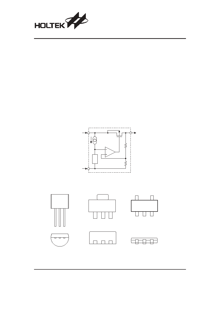
1.5V Low Power LDO
Block Diagram
Pin Assignment
Note:
For lead free devices, TO-92 package will add a
≤#≤ mark at the end of the date code, whereas SOT-89 and
SOT-25 packages will add a
≤#≤ mark at the end of the marking.
Rev. 1.10
1
March 13, 2006
Applications
∑
Battery-powered equipment
∑
Communication equipment
∑
Audio/Video equipment
General Description
The HT1015-1 is a three-terminal low power voltage regu-
lator implemented in CMOS technology. It is available with
a fixed output voltage at 1.5V. CMOS technology ensures
low voltage drop and low quiescent current.
Although designed primarily as a fixed voltage regulator,
this device can be used with external components to ob-
tain variable voltages and currents.
Features
∑
Low power consumption
∑
Low voltage drop
∑
Low temperature coefficient
∑
Wide operating voltage (12V max.)
∑
TO-92, SOT-89 and SOT-25 package
VOUT
VIN
GND
Vref
1 0 1 5 - 1
F r o n t V i e w
B o t t o m V i e w
V O U T
G N D
V I N
T O - 9 2
G N D
V I N
V O U T
S O T - 8 9
G N D
V I N
V O U T
1 0 1 5 - 1
N C
N C
T o p V i e w
S O T - 2 5
0 1 5 1
G N D
V I N
V O U T
G N D
V I N
V O U T

Absolute Maximum Ratings
Supply Voltage ............................V
SS
-0.3V to V
SS
+13V
Storage Temperature ............................
-50∞C to 125∞C
Power Consumption (*1) ...................................200mW
Operating Temperature...........................
-40∞C to 85∞C
Power Consumption (*2) ...................................150mW
Note: These are stress ratings only. Stresses exceeding the range specified under
≤Absolute Maximum Ratings≤ may
cause substantial damage to the device. Functional operation of this device at other conditions beyond those
listed in the specification is not implied and prolonged exposure to extreme conditions may affect device reliabil-
ity.
*1: applied to SOT-89 and TO-92
*2: applied to SOT-25
Electrical Characteristics
Ta=25
∞C
Symbol
Parameter
Test Conditions
Min.
Typ.
Max.
Unit
V
IN
Conditions
V
OUT
Output Voltage Tolerance
3.5V
I
OUT
=0.5mA
1.455
1.5
1.545
V
I
OUT
Output Current
3.5V
æ
7.0
18
æ
mA
DV
OUT
Load Regulation
3.5V
1mA
£I
OUT
£7mA
æ
15
æ
mV
V
DIF
Voltage Drop
æ
I
OUT
=0.5mA
æ
250
æ
mV
I
SS
Current Consumption
3.5V
No load
æ
2.2
5.0
mA
V
V xV
OUT
IN
OUT
Line Regulation
æ
2.5V
£V
IN
£12V
I
OUT
=0.5mA
æ
0.1
æ
%/V
V
IN
Input Voltage
æ
æ
æ
æ
12
V
V
Ta
OUT
Temperature Coefficient
3.5V
I
OUT
=0.5mA
-40∞C~85∞C
æ
-0.75
æ
mV/
∞C
HT1015-1
Rev. 1.10
2
March 13, 2006
D
D
D
D

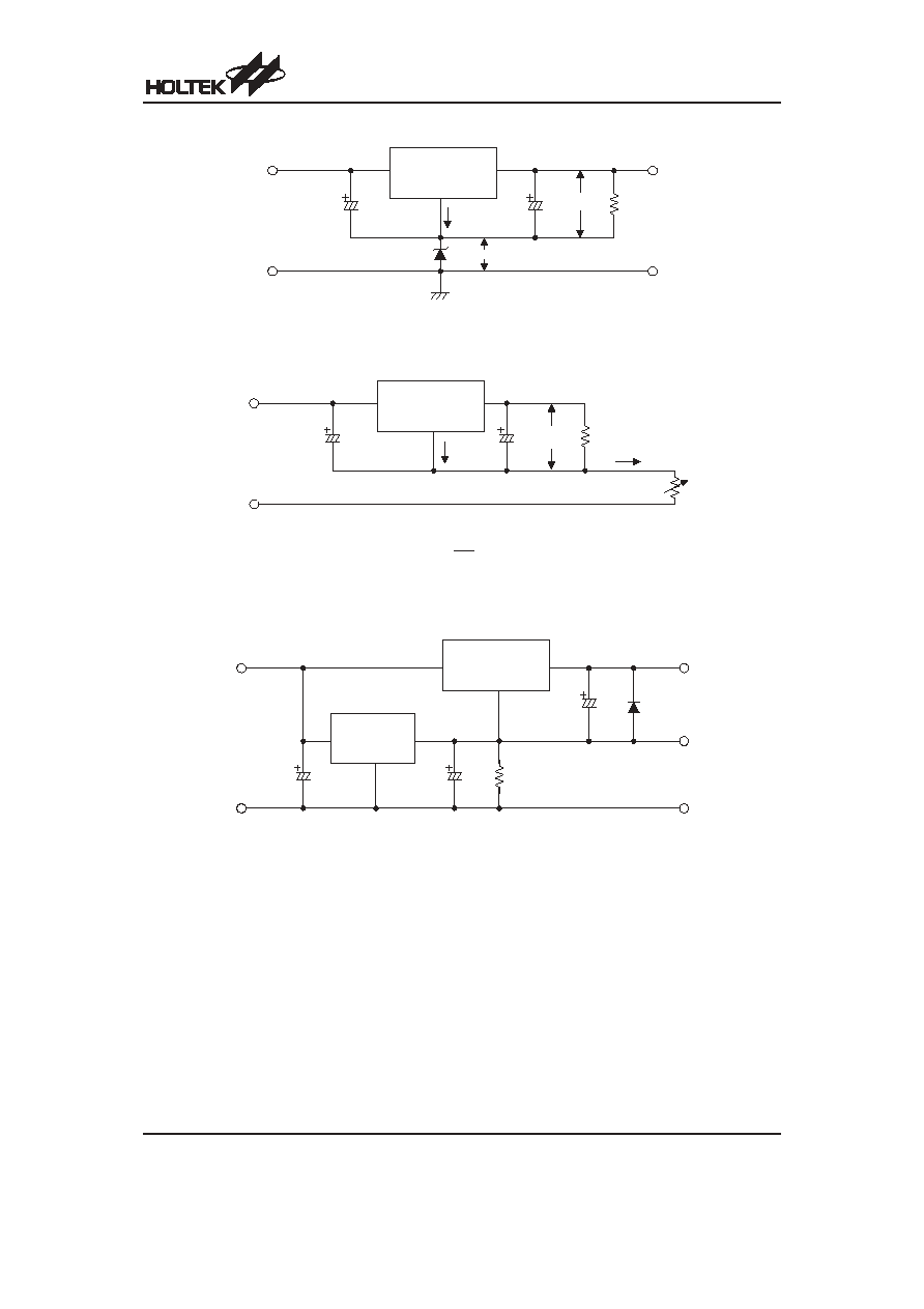
Application Circuits
Basic Circuit
High Output Current Positive Voltage Regulator
Short-Circuit Protection Using External Transistors
Increased Output Voltage Circuits
V
= V
( 1 +
R2
R1
) + I R2
OUT1
XX
SS
HT1015-1
Rev. 1.10
3
March 13, 2006
H T 1 0 1 5 - 1
C 1
1 0 m F
C 2
1 0 m F
C o m m o n
C o m m o n
S i n g l e p o i n t G N D
G N D
V
I N
V
O U T
V
O U T
V
I N
C o m m o n
C o m m o n
S i n g l e p o i n t G N D
G N D
T r 1
R s
R 1
H T 1 0 1 5 - 1
V
I N
V
O U T
V
I N
V
O U T
C 1
1 0 m F
C 2
1 0 m F
T r 2
C o m m o n
C o m m o n
S i n g l e p o i n t G N D
G N D
R 1
T r 1
H T 1 0 1 5 - 1
V
I N
V
I N
V
O U T
V
O U T
C 1
1 0 m F
C 2
1 0 m F
C o m m o n
C o m m o n
S i n g l e p o i n t G N D
G N D
R 1
R 2
H T 1 0 1 5 - 1
V
I N
V
O U T
V
I N
V
O U T 1
V
X X
I
S S
C 1
1 0 m F
C 2
1 0 m F
V
= V
+ V
OUT1
XX
D1
Constant Current Regulator
I
=
V
R
+ I
OUT
XX
A
SS
Dual Supply
HT1015-1
Rev. 1.10
4
March 13, 2006
C o m m o n
C o m m o n
S i n g l e p o i n t G N D
G N D
D 1
R 1
V
X X
H T 1 0 1 5 - 1
V
I N
V
O U T
V
I N
V
O U T 1
I
S S
C 1
1 0 m F
C 2
1 0 m F
V
D 1
C o m m o n
G N D
V
X X
I
S S
H T 1 0 1 5 - 1
V
I N
V
O U T
R
A
V
I N
I
O U T
R
L
C 1
1 0 m F
C 2
1 0 m F
G N D
I C 1
G N D
I C 2
C o m m o n
C o m m o n
R 1
V
I N
V
O U T
V
I N
V
O U T
V
I N
V
O U T 1
V
O U T 2
C 1
1 0 m F
C 2
1 0 m F
C 3
1 0 m F
H T 1 0 1 5 - 1
H T 1 0 1 5 - 1

Package Information
3-pin TO-92 Outline Dimensions
Symbol
Dimensions in mil
Min.
Nom.
Max.
A
170
æ
200
B
170
æ
200
C
500
æ
æ
D
11
æ
20
E
90
æ
110
F
45
æ
55
G
45
æ
65
H
130
æ
160
I
8
æ
18
a
4
∞
æ
6
∞
HT1015-1
Rev. 1.10
5
March 13, 2006
A
B
C
E
F
G
H
D