 | –≠–ª–µ–∫—Ç—Ä–æ–Ω–Ω—ã–π –∫–æ–º–ø–æ–Ω–µ–Ω—Ç: HT1602L | –°–∫–∞—á–∞—Ç—å:  PDF PDF  ZIP ZIP |

HT1602L
40 Dot Matrix LCD Segment Driver
Block Diagram
Features
∑
Operating voltage: 2.7V~5.5V
∑
LCD driving voltage: 3.0V~5.2V
∑
Applicable LCD duty from 1/8 to 1/16
∑
Suitable for various types of LCD panel
∑
Bias voltage adjustable from an external
source
General Description
The HT1602L is a dot matrix LCD segment
driver LSI implemented in CMOS technology.
The chip contains 40-bit shift register (two 20-
bit shift registers), 40-bit latch (two 20-bit
latches), 40-bit level shifter, 40-bit 4-level
driver and control circuits.
The HT1602L can convert serial data received
from an LCD controller parallel data and then
send them out as LCD driving waveforms to the
LCD panel. The chip is applicable up to 1/16
duty. Furthermore, the bias voltage which de-
termines the LCD driving voltage can be option-
ally supplied from an external source, thus the
chip is suitable for driving various LCD panel.
These special features increase the versatility
of the chip.
Applications
∑
Interface with HT163A
∑
Electronic dictionaries
∑
Portable computers
∑
Remote controllers
∑
Calculators
1
27th Aug '98

Pad Assignment
Chip size: 87
◊
74 (mil)
2
* The IC substrate should be connected to VSS in the PCB layout artwork.
Pad Coordinates
Unit:
µ
m
Pad No.
X
Y
Pad No.
X
Y
1
≠975.00
780.00
28
975.00
≠713.00
2
≠975.00
650.00
29
975.00
≠583.00
3
≠975.00
520.00
30
942.50
≠435.50
4
≠975.00
390.00
31
942.50
≠305.50
5
≠975.00
260.00
32
942.50
≠175.50
6
≠975.00
130.00
33
975.00
≠45.50
7
≠975.00
0.00
34
923.50
84.50
8
≠975.00
≠130.00
35
975.00
239.00
9
≠975.00
≠260.00
36
975.00
369.00
10
≠975.00
≠390.00
37
975.00
499.00
11
≠975.00
≠520.00
38
975.00
629.00
12
≠975.00
≠650.00
39
975.00
780.00
13
≠975.00
≠780.00
40
845.00
780.00
14
≠845.00
≠780.00
41
715.00
780.00
15
≠715.00
≠780.00
42
585.00
780.00
16
≠585.00
≠780.00
43
455.00
780.00
HT1602L
2
27th Aug '98

Pad No.
X
Y
Pad No.
X
Y
17
≠455.00
≠780.00
44
325.00
780.00
18
≠325.00
≠780.00
45
195.00
780.00
19
≠195.00
≠780.00
46
65.00
780.00
20
≠65.00
≠780.00
47
≠65.00
780.00
21
65.00
≠780.00
48
≠195.00
780.00
22
195.00
≠780.00
49
≠325.00
780.00
23
325.00
≠780.00
50
≠455.00
780.00
24
455.00
≠780.00
51
≠585.00
780.00
25
585.00
≠780.00
52
≠715.00
780.00
26
715.00
≠780.00
53
≠845.00
780.00
27
845.00
≠780.00
Pad Description
Pad No.
Pad Name
I/O
Description
1~5
Y15~Y19
O
LCD driver output for segment*
6
VDD
--
Power supply (postive)
7~26
Y20~Y39
O
LCD driver output for segment
27
DO39
O
Shift register output pad for the 40th bit data
28
DI20
I
Data input pad of shift register 2
29
DO19
O
Shift register output pad for the 20th bit data
30, 31, 32
V5, V3, V2
I
LCD bias supply voltage
33
VSS
--
Power supply (ground)
34
VDD
--
Power supply (positive)
35
CLK
I
Clock pulse input pad for the shift register
36
DI0
I
Data input pad of shift register 1
37
LOAD
I
Latching signal to latch shift register data
38
ALT
I
Alternate signal input pad for LCD driving waveform
39~53
Y0~Y14
O
LCD driver output for segment*
*: For Y0~Y39, one of VDD, V2, V3 or V5 is selected as a display driving source according to the
combination of latched data level and ALT signal. Refer to the following table:
Latched Data
ALT
Display data output level
H
H
V5
L
V
DD
L
H
V3
L
V2
HT1602L
3
27th Aug '98

Absolute Maximum Ratings*
Supply Voltage .............................. ≠0.3V to 6.0V
Storage Temperature................. ≠50
∞
C to 125
∞
C
Input Voltage................. V
SS
≠0.3V to V
DD
+0.3V
Operating Temperature............... ≠20
∞
C to 70
∞
C
*Note: These are stress ratings only. Stresses exceeding the range specified under "Absolute Maxi-
mum Ratings" may cause substantial damage to the device. Functional operation of this
device at other conditions beyond those listed in the specification is not implied and prolonged
exposure to extreme conditions may affect device reliability.
D.C. Characteristics
Ta=25
∞
C
Symbol
Parameter
Test Conditions
Min.
Typ.
Max.
Unit
V
DD
Conditions
V
DD
Operating Voltage
--
--
2.7
--
5.5
V
I
OP
Operating Current
5V
No load
--
100
300
µ
A
I
DD
Standby Current
5V
--
--
1
5
µ
A
f
LCD
Clock Frequency
5V
--
3.3
--
--
MHz
tw
CLK
Clock Pulse Width
5V
--
125
--
--
ns
V
IL
"L" Input Voltage
5V
--
--
--
0.3VDD
V
V
IH
"H" Input Voltage
5V
--
0.7VDD
--
--
V
V
LCD
LCD Driving Voltage
5V
--
3
--
5.2
V
HT1602L
4
27th Aug '98
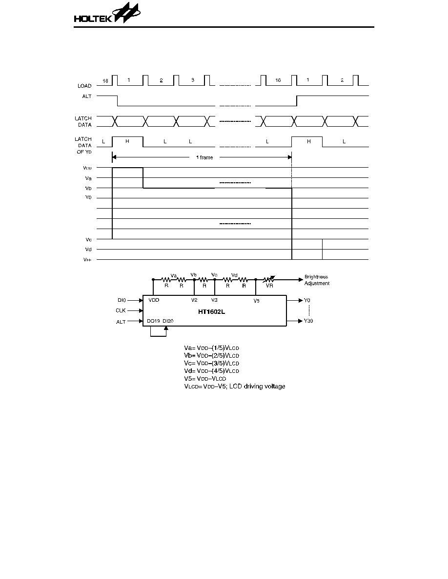
Timing Diagrams
1/16 duty and 1/5 bias
HT1602L
5
27th Aug '98
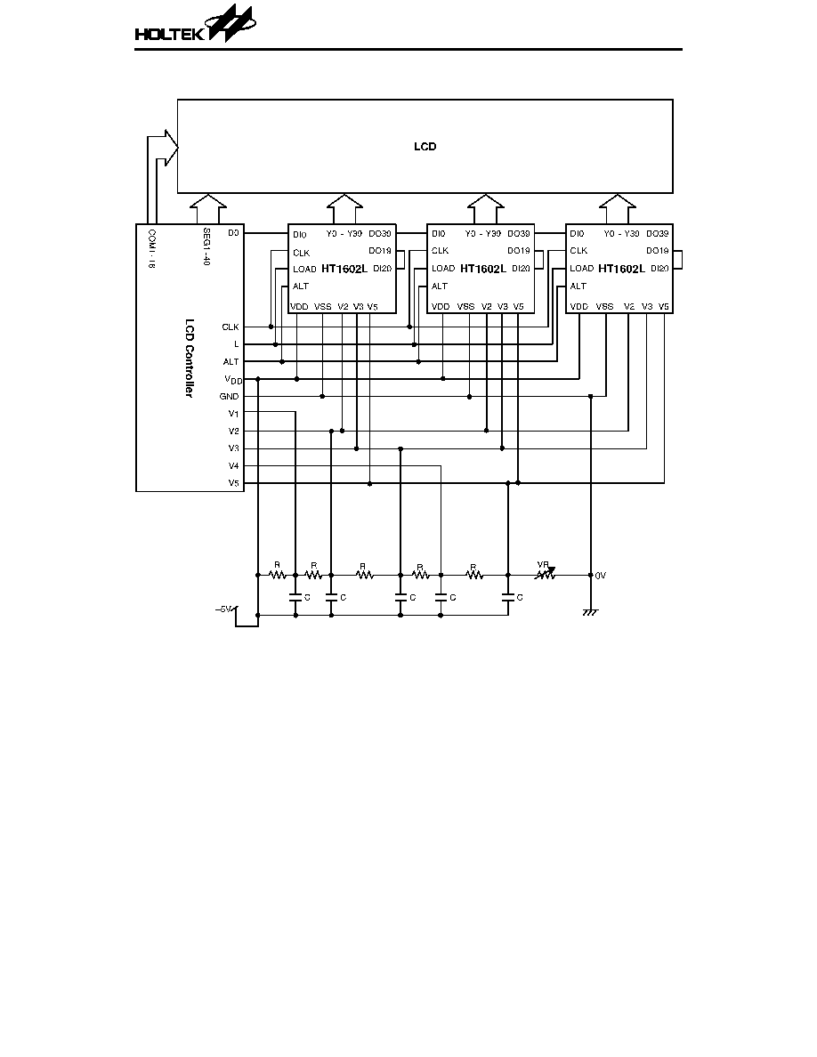
Application Circuits
HT1602L
6
27th Aug '98