 | –≠–ª–µ–∫—Ç—Ä–æ–Ω–Ω—ã–π –∫–æ–º–ø–æ–Ω–µ–Ω—Ç: HT46CU25 | –°–∫–∞—á–∞—Ç—å:  PDF PDF  ZIP ZIP |

HT46RU25/HT46CU25
A/D Type 8-Bit MCU
I
2
C is a trademark of Philips Semiconductors.
Rev. 1.00
1
July 10, 2006
General Description
The HT46RU25/HT46CU25 are 8-bit, high perfor-
mance, RISC architecture microcontroller devices spe-
cifically designed for A/D applications that interface
directly to analog signals, such as those from sensors.
The mask version HT46CU25 is fully pin and function-
ally compatible with the OTP version HT46RU25 de-
vice.
The advantages of low power consumption, I/O flexibil-
ity, programmable frequency divider, timer functions,
oscillator options, multi-channel A/D Converter, Pulse
Width Modulation function, UART function, I
2
C inter-
face, HALT and wake-up functions, enhance the versa-
tility of these devices to suit a wide range of A/D
application possibilities such as sensor signal process-
ing, motor driving, industrial control, consumer prod-
ucts, subsystem controllers, etc.
The HT46CU25 is under development and will be avail-
able soon.
Features
∑
Operating voltage:
f
SYS
=4MHz: 2.2V~5.5V
f
SYS
=8MHz: 3.3V~5.5V
∑
System clock (f
SYS
): 400kHz~8MHz, 32.768kHz
∑
48 bidirectional I/O lines (max.)
∑
One interrupt input shared with an I/O line
∑
One 8-bit and two 16-bit programmable timer/event
counter with prescaler and PFD (programmable
frequency divider) function and overflow interrupt
∑
16K
¥16 program memory in two banks (Bank 0, 1)
∑
576
¥8 (192¥3) data memory RAM
(address from 040H~0FFH, bank 0~2)
∑
On-chip crystal and RC oscillator
∑
Watchdog Timer
∑
Supports PFD for sound generation
∑
Real Time Clock (RTC) with 8-bit prescaler
∑
HALT function and wake-up feature reduce power
consumption
∑
Up to 0.5
ms instruction cycle with 8MHz system clock
at V
DD
=5V
∑
16-level subroutine nesting
∑
8-channels 12-bit resolution A/D converter
∑
4-channels (6+2)/(7+1)-bit PWM output shared with
four I/O lines
∑
Universal Asynchronous Receiver Transmitter
(UART)
∑
Bit manipulation instruction
∑
16-bit table read instruction
∑
63 powerful instructions
∑
All instructions in one or two machine cycles
∑
Low voltage reset function
∑
I
2
C Bus (slave mode)
∑
48/56-pin SSOP package
Technical Document
∑
Tools Information
∑
FAQs
∑
Application Note
-
HA0004E HT48 & HT46 MCU UART Software Implementation Method
-
HA0005E Controlling the I2C bus with the HT48 & HT46 MCU Series
-
HA0013E HT48 & HT46 LCM Interface Design
-
HA0047E An PWM application example using the HT46 series of MCUs
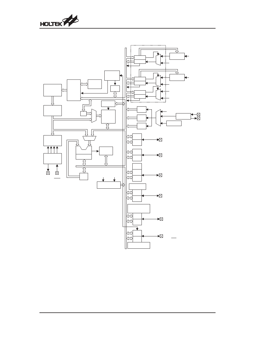
Block Diagram
HT46RU25/HT46CU25
Rev. 1.00
2
July 10, 2006
O S C 2
O S C 4
O S C 1
R E S
V D D
M U X
V S S
O S C 3
P r o g r a m
E P R O M
P r o g r a m
C o u n t e r
I n t e r r u p t
C i r c u i t
S T A C K
I N T C
D A T A
M e m o r y
I n s t r u c t i o n
R e g i s t e r
M
U
X
I n s t r u c t i o n
D e c o d e r
S T A T U S
A L U
S h i f t e r
T i m i n g
G e n e r a t o r
A C C
M P
L V R
H A L T
E N / D I S
M
U
X
W D T
M
U
X
P F D 0
P F D 1
f
S Y S
/ 4
f
S Y S
P r e s c a l e r
T M R 0
P D C
P D
P D 0 / P W M 0 ~ P D 3 / P W M 3
P D 4 ~ P D 7
P B
P B C
P B 0 / A N 0 ~ P B 7 / A N 7
P W M
8 - C h a n n e l
A / D C o n v e r t e r
T M R 1
P F
P F C
P A C
P A 0 ~ P A 2
P A 3 / P F D
P A 4
P A 5 / I N T
P A 6 / S D A
P A 7 / S C L
I
2
C B u s
S l a v e M o d e
P C
P C C
P C 0 / T X
P C 1 / R X
P C 2 ~ P C 5
P C 6 / O S C 3
P C 7 / O S C 4
B P
P A 5
P o r t F
P F 0 ~ P F 7
P o r t D
P o r t C
P o r t B
P o r t A
M
U
X
W D T O S C
f
S Y S
/ 4
T M R 0 C
T M R 0
T M R 1 C
T M R 1
M
U
X
f
S Y S
P r e s c a l e r
T M R 2
T M R 2 C
T M R 2
T i m e
B a s e
R T C
W D T O S C
U A R T B u s
P A
P G
P G C
P o r t G
P G 0 ~ P G 7
O S C 3
O S C 4

Pin Assignment
HT46RU25/HT46CU25
Rev. 1.00
3
July 10, 2006
H T 4 6 R U 2 5 / H T 4 6 C U 2 5
4 8 S S O P - A
4 8
4 7
4 6
4 5
4 4
4 3
4 2
4 1
4 0
3 9
3 8
3 7
3 6
3 5
3 4
3 3
3 2
3 1
3 0
2 9
2 8
2 7
2 6
2 5
1
2
3
4
5
6
7
8
9
1 0
1 1
1 2
1 3
1 4
1 5
1 6
1 7
1 8
1 9
2 0
2 1
2 2
2 3
2 4
P B 5 / A N 5
P B 4 / A N 4
P A 3 / P F D
P A 2
P A 1
P A 0
P B 3 / A N 3
P B 2 / A N 2
P B 1 / A N 1
P B 0 / A N 0
T M R 2
P F 3
P F 2
P F 1
P D 7
P D 6
P D 5
P D 4
V S S
P F 0
T M R 0
P C 0 / T X
P C 1 / R X
P C 2
P B 6 / A N 6
P B 7 / A N 7
P A 4
P A 5 / I N T
P A 6 / S D A
P A 7 / S C L
P F 4
P F 5
P F 6
P F 7
O S C 2
O S C 1
V D D
R E S
T M R 1
P D 3 / P W M 3
P D 2 / P W M 2
P D 1 / P W M 1
P D 0 / P W M 0
P C 7 / O S C 4
P C 6 / O S C 3
P C 5
P C 4
P C 3
H T 4 6 R U 2 5 / H T 4 6 C U 2 5
5 6 S S O P - A
5 6
5 5
5 4
5 3
5 2
5 1
5 0
4 9
4 8
4 7
4 6
4 5
4 4
4 3
4 2
4 1
4 0
3 9
3 8
3 7
3 6
3 5
3 4
3 3
3 2
3 1
3 0
2 9
1
2
3
4
5
6
7
8
9
1 0
1 1
1 2
1 3
1 4
1 5
1 6
1 7
1 8
1 9
2 0
2 1
2 2
2 3
2 4
2 5
2 6
2 7
2 8
P B 5 / A N 5
P B 4 / A N 4
P A 3 / P F D
P A 2
P A 1
P A 0
P B 3 / A N 3
P B 2 / A N 2
P B 1 / A N 1
P B 0 / A N 0
T M R 2
P F 3
P F 2
P F 1
P D 7
P D 6
P D 5
P D 4
V S S
P F 0
T M R 0
P C 0 / T X
P C 1 / R X
P C 2
P G 0
P G 1
P G 2
P G 3
P B 6 / A N 6
P B 7 / A N 7
P A 4
P A 5 / I N T
P A 6 / S D A
P A 7 / S C L
P F 4
P F 5
P F 6
P F 7
O S C 2
O S C 1
V D D
R E S
T M R 1
P D 3 / P W M 3
P D 2 / P W M 2
P D 1 / P W M 1
P D 0 / P W M 0
P C 7 / O S C 4
P C 6 / O S C 3
P C 5
P C 4
P C 3
P G 7
P G 6
P G 5
P G 4
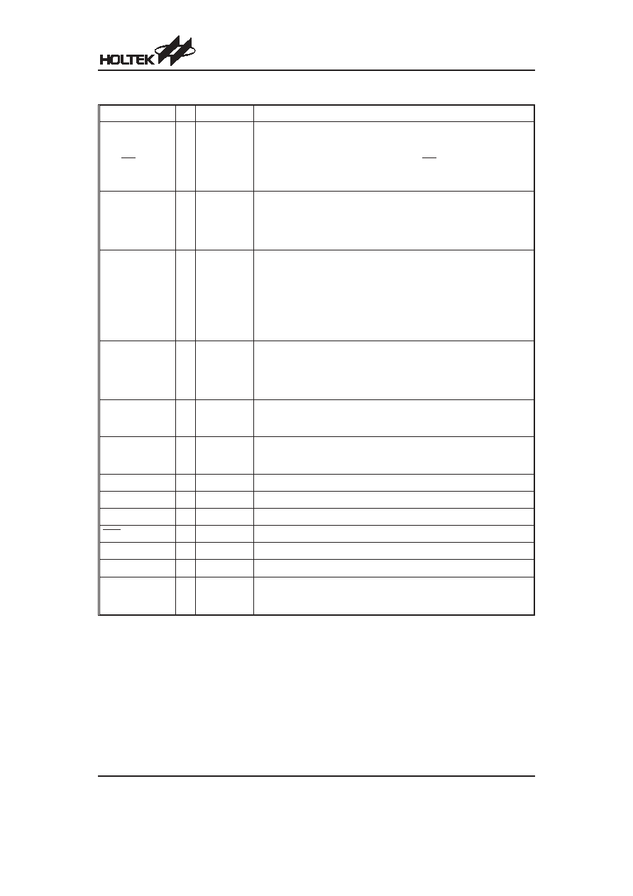
Pin Description
Pin Name
I/O
Options
Description
PA0~PA2
PA3/PFD
PA4
PA5/INT
PA6/SDA
PA7/SCL
I/O
Pull-high
Wake-up
PA3 or PFD
I/O or I
2
C Bus
Bidirectional 8-bit input/output port. Each bit can be configured as wake-up
input by option (bit option). Software instructions determine the CMOS out-
put or Schmitt trigger input with or without pull-high resistor (determine by
pull-high options: bit option). The PFD and INT are pin-shared with PA3
and PA5, respectively. Once the I
2
C Bus function is used, the internal reg-
isters related to PA6 and PA7 cannot be used.
PB0/AN0~
PB7/AN7
I/O
Pull-high
Bidirectional 8-bit input/output port. Software instructions determine the
CMOS output, Schmitt trigger input with or without pull-high resistor (deter-
mined by pull-high option: bit option) or A/D input. Once a PB line is se-
lected as an A/D input (by using software control), the I/O function and
pull-high resistor are automatically disabled.
PC0/TX
PC1/RX
PC2~PC5
PC6/OSC3
PC7/OSC4
I/O
Pull-high
I/O or UART
OSC3/OSC4
Bidirectional 8-bit input/output port. Software instructions determine the
CMOS output, Schmitt trigger input with or without pull-high resistor (deter-
mine by pull-high option: byte option).
TX and RX are pin-shared with PC0 and PC1, once the UART Bus function
is used, the internal registers related to PC0 and PC1 cannot be used.
Software instructions determine the UART function to be used.
OSC3/OSC4 are pin shared with PC6/PC7. (depending on the OSC type
option)
PD0/PWM0
PD1/PWM1
PD2/PWM2
PD3/PWM3
PD4~PD7
I/O
Pull-high
PWM
Bidirectional 8-bit input/output port. Software instructions determine the
CMOS output, Schmitt trigger input with or without a pull-high resistor (de-
termined by pull-high option: byte option). The PWM0/PWM1/PWM2/
PWM3 output function are pin-shared with PD0/PD1/PD2/PD3 (depending
on the PWM options).
PF0~PF7
I/O
Pull-high
Bidirectional 8-bit input/output port. Software instructions determine the
CMOS output, Schmitt trigger input with or without pull-high resistor (deter-
mine by pull-high option: byte option).
PG0~PG7
(56-pin package only)
I/O
Pull-high
Bidirectional 8-bit input/output port. Software instructions determine the
CMOS output, Schmitt trigger input with or without pull-high resistor (deter-
mine by pull-high option: byte option).
TMR0
I
æ
Timer/Event Counter 0 Schmitt trigger input (without pull-high resistor)
TMR1
I
æ
Timer/Event Counter 1 Schmitt trigger input (without pull-high resistor).
TMR2
I
æ
Timer/Event Counter 2 Schmitt trigger input (without pull-high resistor).
RES
I
æ
Schmitt trigger reset input, active low
VSS
æ
æ
Negative power supply, ground
VDD
æ
æ
Positive power supply
OSC1
OSC2
I
O
Crystal
or RC
OSC1 and OSC2 are connected to an RC network or a crystal (by options)
for the internal system clock. In the case of RC operation, OSC2 is the
output terminal for 1/4 system clock.
Absolute Maximum Ratings
Supply Voltage ...........................V
SS
-0.3V to V
SS
+6.0V
Storage Temperature ............................
-50∞C to 125∞C
Input Voltage..............................V
SS
-0.3V to V
DD
+0.3V
Operating Temperature...........................
-40∞C to 85∞C
Note: These are stress ratings only. Stresses exceeding the range specified under
≤Absolute Maximum Ratings≤ may
cause substantial damage to the device. Functional operation of this device at other conditions beyond those
listed in the specification is not implied and prolonged exposure to extreme conditions may affect device reliabil-
ity.
HT46RU25/HT46CU25
Rev. 1.00
4
July 10, 2006
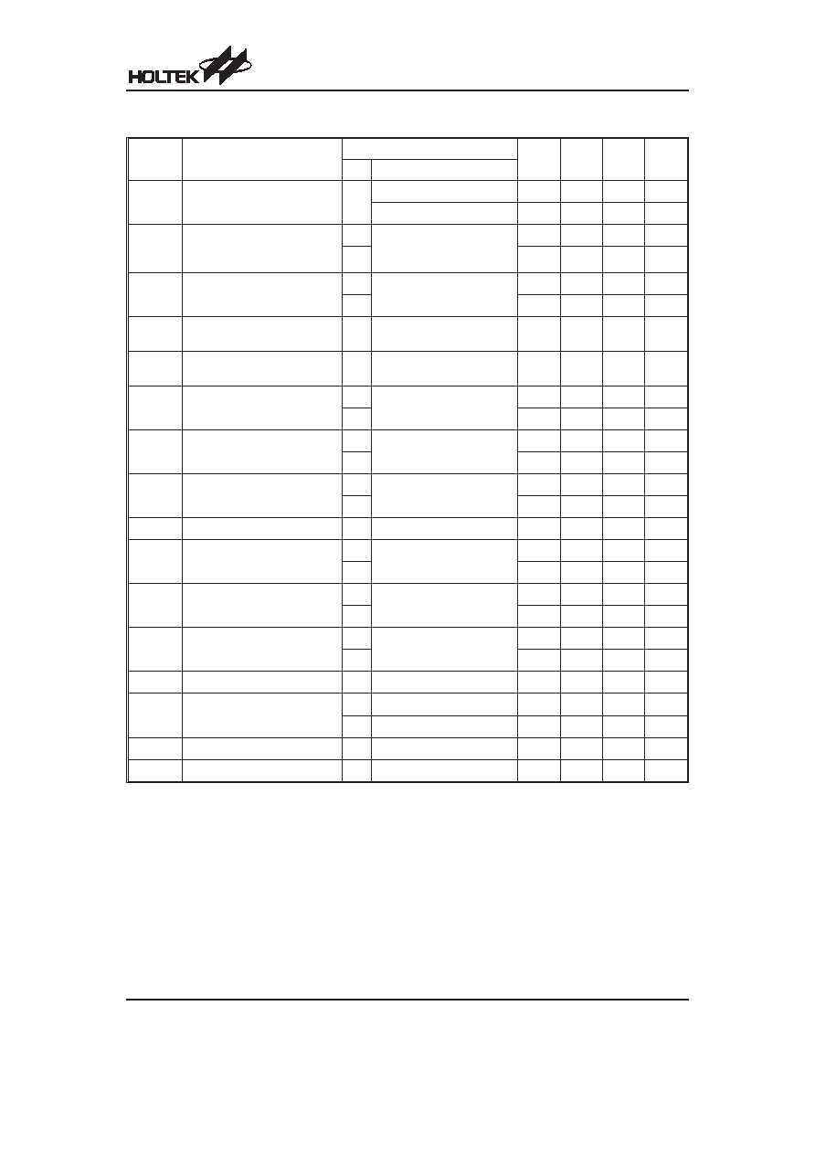
D.C. Characteristics
Ta=25
∞C
Symbol
Parameter
Test Conditions
Min.
Typ.
Max.
Unit
V
DD
Conditions
V
DD
Operating Voltage
æ
f
SYS
=4MHz
2.2
æ
5.5
V
f
SYS
=8MHz
3.3
æ
5.5
V
I
DD1
Operating Current
(Crystal OSC, RC OSC)
3V
No load, f
SYS
=4MHz,
ADC Off,
UART Off
æ
1
2
mA
5V
æ
2.5
5
mA
I
DD2
Operating Current
(Crystal OSC, RC OSC)
3V
No load, f
SYS
=4MHz,
ADC Off, UART On
æ
2
4
mA
5V
æ
5
10
mA
I
DD3
Operating Current
(Crystal OSC, RC OSC)
5V
No load, f
SYS
=8MHz,
ADC Off, UART Off
æ
4
8
mA
I
DD4
Operating Current
(Crystal OSC, RC OSC)
5V
No load, f
SYS
=8MHz,
ADC Off, UART On
æ
6
12
mA
I
DD5
Operating Current
(f
SYS
=RTC OSC)
3V
No load, ADC Off,
UART Off
æ
0.3
0.6
mA
5V
æ
0.6
1
mA
I
STB1
Standby Current
(WDT Enabled)
3V
No load, system HALT,
UART Off
æ
æ
5
mA
5V
æ
æ
10
mA
I
STB2
Standby Current
(WDT Disabled)
3V
No load, system HALT,
UART Off
æ
æ
1
mA
5V
æ
æ
2
mA
V
LVR
Low Voltage Reset Voltage
æ
æ
2.7
3
3.3
V
I
OL
I/O Port Sink Current
3V
V
OL
=0.1V
DD
4
8
æ
mA
5V
10
20
æ
mA
I
OH
I/O Port Source Current
3V
V
OH
=0.9V
DD
-2
-4
æ
mA
5V
-5
-10
æ
mA
R
PH
Pull-high Resistance
3V
æ
20
60
100
k
W
5V
10
30
50
k
W
V
AD
A/D Input Voltage
æ
æ
0
æ
V
DD
V
I
ADC
Additional Power Consumption
if A/D Converter is Used
3V
No load
æ
0.5
1
mA
5V
No load
æ
1.5
3
mA
DNL
ADC Differential Non-Linear
æ
æ
æ
æ
±2
LSB
INL
ADC Integral Non-Linear
æ
æ
æ
±2.5
±4
LSB
HT46RU25/HT46CU25
Rev. 1.00
5
July 10, 2006