 | ÐлекÑÑоннÑй компоненÑ: HT46R64 | СкаÑаÑÑ:  PDF PDF  ZIP ZIP |
Äîêóìåíòàöèÿ è îïèñàíèÿ www.docs.chipfind.ru

HT46R64/HT46C64
A/D with LCD Type 8-Bit MCU
Rev. 1.40
1
September 21, 2004
Features
·
Operating voltage:
f
SYS
=4MHz: 2.2V~5.5V
f
SYS
=8MHz: 3.3V~5.5V
·
24 bidirectional I/O lines
·
Two external interrupt input
·
One 8-bit and one 16-bit programmable timer/event
counter with PFD (programmable frequency divider)
function
·
LCD driver with 33
´3 or 32´4 segments
(logical output option for SEG0~SEG15)
·
4K
´15 program memory
·
192
´8 data memory RAM
·
Supports PFD for sound generation
·
Real Time Clock (RTC)
·
8-bit prescaler for RTC
·
Watchdog Timer
·
Buzzer output
·
On-chip crystal, RC and 32768Hz crystal oscillator
·
HALT function and wake-up feature reduce power
consumption
·
8-level subroutine nesting
·
8 channels 10-bit resolution A/D converter
·
4-channel 8-bit PWM output shared with 4 I/O lines
·
Bit manipulation instruction
·
16-bit table read instruction
·
Up to 0.5
ms instruction cycle with 8MHz system clock
·
63 powerful instructions
·
All instructions in 1 or 2 machine cycles
·
Low voltage reset/detector function
·
56-pin SSOP, 100-pin QFP package
General Description
The HT46R64/HT46C64 are 8-bit, high performance,
RISC architecture microcontroller devices specifically
designed for A/D product applications that interface di-
rectly to analog signals and which require LCD Inter-
face. The mask version HT46C64 is fully pin and
functionally compatible with the OTP version HT46R64
device.
The advantages of low power consumption, I/O flexibil-
ity, timer functions, oscillator options, multi-channel A/D
Converter, Pulse Width Modulation function, HALT and
wake-up functions, in addition to a flexible and
configurable LCD interface enhance the versatility of
these devices to control a wide range of applications re-
quiring analog signal processing and LCD interfacing,
such as electronic metering, environmental monitoring,
handheld measurement tools, motor driving, etc., for
both industrial and home appliance application areas.
HT46C64 under development, available in 4Q, 2004.
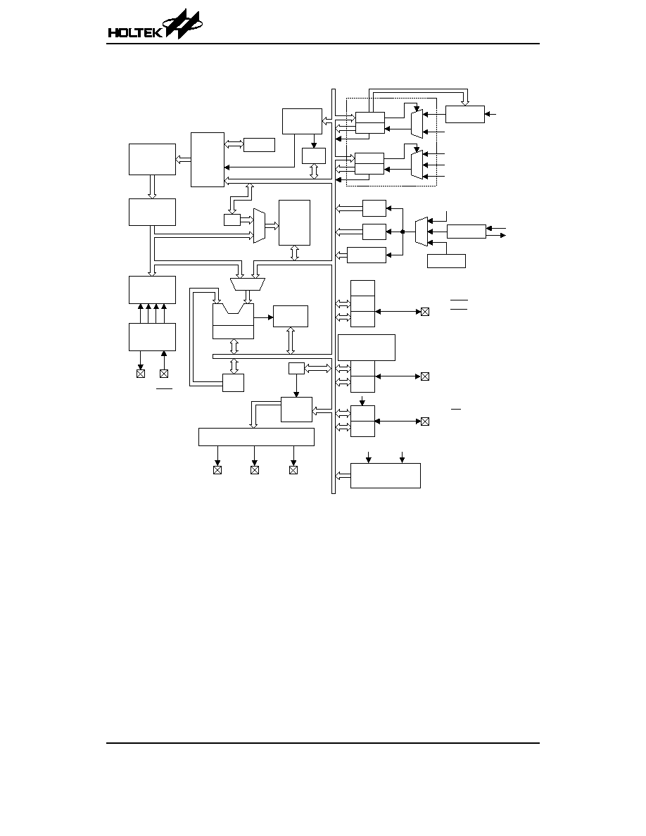
Block Diagram
HT46R64/HT46C64
Rev. 1.40
2
September 21, 2004
P r o g r a m
C o u n t e r
P r o g r a m
E P R O M
I n s t r u c t i o n
R e g i s t e r
I n s t r u c t i o n
D e c o d e r
T i m i n g
G e n e r a t i o n
O S C 2
O S C 4
O S C 1
R E S
V D D
V S S
O S C 3
I n t e r r u p t
C i r c u i t
I N T C
M P
M
U
X
M U X
D A T A
M e m o r y
A L U
S h i f t e r
S T A T U S
A C C
M
U
X
W D T O S C
R T C O S C
O S C 3
O S C 4
R T C
S T A C K
L C D
M e m o r y
B P
L C D D R I V E R
C O M 0 ~
C O M 2
C O M 3 /
S E G 3 2
S E G 0 ~
S E G 3 1
T i m e B a s e
W D T
f
S Y S
/ 4
P A C
P A
P O R T A
P D C
P D
P O R T D
P D 0 / P W M 0 ~ P D 3 / P W M 3
P D 4 / I N T 0
P D 5 / I N T 1
P D 6 / T M R 0
P D 7 / T M R 1
P O R T B
P B
P B C
P B 0 / A N 0 ~ P B 7 / A N 7
P A 0 / B Z
P A 1 / B Z
P A 2
P A 3 / P F D
P A 4 ~ P A 7
P W M
8 - C h a n n e l
A / D C o n v e r t e r
H A L T
E N / D I S
L V D / L V R
T M R 0 C
T M R 0
M
U
X
T M R 1 C
T M R 1
M
U
X
P F D 0
P F D 1
f
S Y S
/ 4
f
S Y S
P r e s c a l e r
P D 6 / T M R 0
3 2 7 6 8 H z
P D 7 / T M R 1
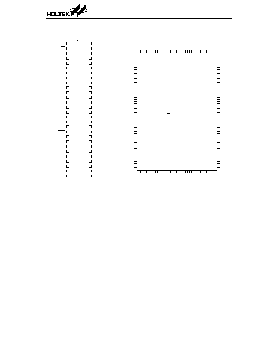
Pin Assignment
HT46R64/HT46C64
Rev. 1.40
3
September 21, 2004
H T 4 6 R 6 4 / H T 4 6 C 6 4
1 0 0 Q F P - A
1
2
3
4
5
6
7
8
9
1 0
1 1
1 2
1 3
1 4
1 5
1 6
1 7
1 8
1 9
2 0
2 1
2 2
2 3
2 4
2 5
2 6
2 7
2 8
2 9
3 0
3 1
3 2 3 3 3 4 3 5 3 6 3 7 3 8 3 9 4 0 4 1 4 2 4 3 4 4 4 5 4 6 4 7 4 8 4 9 5 0
8 1
8 2
8 3
8 4
8 5
8 6
8 7
8 8
8 9
9 0
9 1
9 2
9 3
9 4
9 5
9 6
9 7
9 8
9 9
1 0 0
8 0
7 9
7 8
7 7
7 6
7 5
7 4
7 3
7 2
7 1
7 0
6 9
6 8
6 7
6 6
6 5
6 4
6 3
6 2
6 1
6 0
5 9
5 8
5 7
5 6
5 5
5 4
5 3
5 2
5 1
P A 5
N C
N C
N C
N C
N C
P A 6
P A 7
P B 0 / A N 0
P B 1 / A N 1
P B 2 / A N 2
P B 3 / A N 3
P B 4 / A N 4
P B 5 / A N 5
P B 6 / A N 6
P B 7 / A N 7
V S S
P D 0 / P W M 0
P D 1 / P W M 1
P D 2 / P W M 2
P D 3 / P W M 3
P D 4 / I N T 0
P D 5 / I N T 1
P D 6 / T M R 0
P D 7 / T M R 1
N C
N C
N C
N C
N C
S
E
G
2
2
S
E
G
2
3
S
E
G
2
4
S
E
G
2
5
S
E
G
2
6
S
E
G
2
7
S
E
G
2
8
S
E
G
2
9
S
E
G
3
0
S
E
G
3
1
C
O
M
3
/
S
E
G
3
2
C
O
M
2
C
O
M
1
C
O
M
0
C
2
C
1
V
2
V
1
V
M
A
X
V
L
C
D
S E G 1
S E G 2
S E G 3
N C
N C
N C
S E G 4
S E G 5
S E G 6
S E G 7
S E G 8
S E G 9
S E G 1 0
S E G 1 1
S E G 1 2
S E G 1 3
S E G 1 4
S E G 1 5
S E G 1 6
S E G 1 7
S E G 1 8
S E G 1 9
S E G 2 0
S E G 2 1
N C
N C
N C
N C
N C
N C
S
E
G
0
N
C
N
C
N
C
N
C
N
C
N
C
N
C
N
C
O
S
C
4
O
S
C
3
V
D
D
O
S
C
2
O
S
C
1
R
E
S
P
A
0
/
B
Z
P
A
1
/
B
Z
P
A
2
P
A
3
/
P
F
D
P
A
4
5 6
5 5
5 4
5 3
5 2
5 1
5 0
4 9
4 8
4 7
4 6
4 5
4 4
4 3
4 2
4 1
4 0
3 9
3 8
3 7
3 6
3 5
3 4
3 3
3 2
3 1
3 0
2 9
1
2
3
4
5
6
7
8
9
1 0
1 1
1 2
1 3
1 4
1 5
1 6
1 7
1 8
1 9
2 0
2 1
2 2
2 3
2 4
2 5
2 6
2 7
2 8
H T 4 6 R 6 4 / H T 4 6 C 6 4
5 6 S S O P - A
P A 0 / B Z
P A 1 / B Z
P A 2
P A 3 / P F D
P A 4
P A 5
P A 6
P A 7
P B 0 / A N 0
P B 1 / A N 1
P B 2 / A N 2
P B 3 / A N 3
P B 4 / A N 4
P B 5 / A N 5
V S S
P D 0 / P W M 0
P D 1 / P W M 1
P D 2 / P W M 2
P D 4 / I N T 0
P D 5 / I N T 1
P D 6 / T M R 0
V L C D
V M A X
V 1
V 2
C 1
C 2
C O M 0
R E S
O S C 1
O S C 2
V D D
O S C 3
O S C 4
S E G 8
S E G 9
S E G 1 0
S E G 1 1
S E G 1 2
S E G 1 3
S E G 1 4
S E G 1 5
S E G 1 6
S E G 1 7
S E G 1 8
S E G 1 9
S E G 2 0
S E G 2 1
S E G 2 2
S E G 2 3
S E G 2 4
S E G 2 5
S E G 2 6
C O M 3 / S E G 3 2
C O M 2
C O M 1
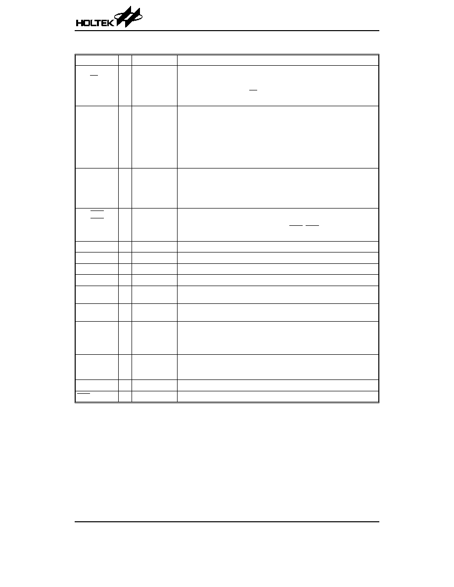
Pin Description
Pin Name
I/O
Options
Description
PA0/BZ
PA1/BZ
PA2
PA3/PFD
PA4~PA7
I/O
Wake-up
Pull-high
Buzzer
PFD
Bidirectional 8-bit input/output port. Each bit can be configured as wake-up in-
put by option. Software instructions determine the CMOS output or Schmitt
Trigger input with or without pull-high resistor (determined by pull-high op-
tions: bit option). The BZ, BZ and PFD are pin-shared with PA0, PA1 and
PA3, respectively.
PB0/AN0
PB1/AN1
PB2/AN2
PB3/AN3
PB4/AN4
PB5/AN5
PB6/AN6
PB7/AN7
I/O
Pull-high
Bidirectional 8-bit input/output port. Software instructions determine the
CMOS output, Schmitt trigger input with or without pull-high resistor (deter-
mined by pull-high option: bit option) or A/D input. Once a PB line is selected
as an A/D input (by using software control), the I/O function and pull-high re-
sistor are disabled automatically.
PD0/PWM0
PD1/PWM1
PD2/PWM2
PD3/PWM3
I/O
Pull-high
PWM
Bidirectional 4-bit input/output port. Software instructions determine the
CMOS output, Schmitt trigger input with or without a pull-high resistor (deter-
mined by pull-high option: bit option). The PWM0/PWM1/PWM2/PWM3 out-
put function are pin-shared with PD0/PD1/PD2/PD3 (dependent on PWM
options).
PD4/INT0
PD5/INT1
PD6/TMR0
PD7/TMR1
I/O
Pull-high
Bidirectional 4-bit input/output port. Software instructions determine the
CMOS output, Schmitt trigger input with or without a pull-high resistor (deter-
mined by pull-high option: bit option). The INT0, INT1, TMR0 and TMR1 are
pin-shared with PD4/PD5/PD6/PD7.
VSS
¾
¾
Negative power supply, ground
VLCD
I
¾
LCD power supply
VMAX
I
¾
IC maximum voltage connect to VDD, VLCD or V1
V1, V2, C1, C2
I
¾
Voltage pump
COM0~COM2
COM3/SEG32
O
1/3 or 1/4 Duty
SEG32 can be set as a segment or as a common output driver for LCD panel
by options. COM0~COM2 are outputs for LCD panel plate.
SEG0~SEG31
O
Logical Output
LCD driver outputs for LCD panel segments. SEG0~SEG23 can be optioned
as logical outputs.
OSC1
OSC2
I
O
Crystal or RC
OSC1 and OSC2 are connected to an RC network or a crystal (by options) for
the internal system clock. In the case of RC operation, OSC2 is the output ter-
minal for 1/4 system clock. The system clock may come from the RTC oscilla-
tor. If the system clock comes from RTCOSC, these two pins can be floating.
OSC3
OSC4
I
O
RTC or
System Clock
Real time clock oscillators. OSC3 and OSC4 are connected to a 32768Hz
crystal oscillator for timing purposes or to a system clock source (depending
on the options). No built-in capacitor
VDD
¾
¾
Positive power supply
RES
I
¾
Schmitt trigger reset input, active low
Absolute Maximum Ratings
Supply Voltage ...........................V
SS
-0.3V to V
SS
+6.0V
Storage Temperature ............................
-50°C to 125°C
Input Voltage..............................V
SS
-0.3V to V
DD
+0.3V
Operating Temperature...........................
-40°C to 85°C
Note: These are stress ratings only. Stresses exceeding the range specified under
²Absolute Maximum Ratings² may
cause substantial damage to the device. Functional operation of this device at other conditions beyond those
listed in the specification is not implied and prolonged exposure to extreme conditions may affect device reliabil-
ity.
HT46R64/HT46C64
Rev. 1.40
4
September 21, 2004
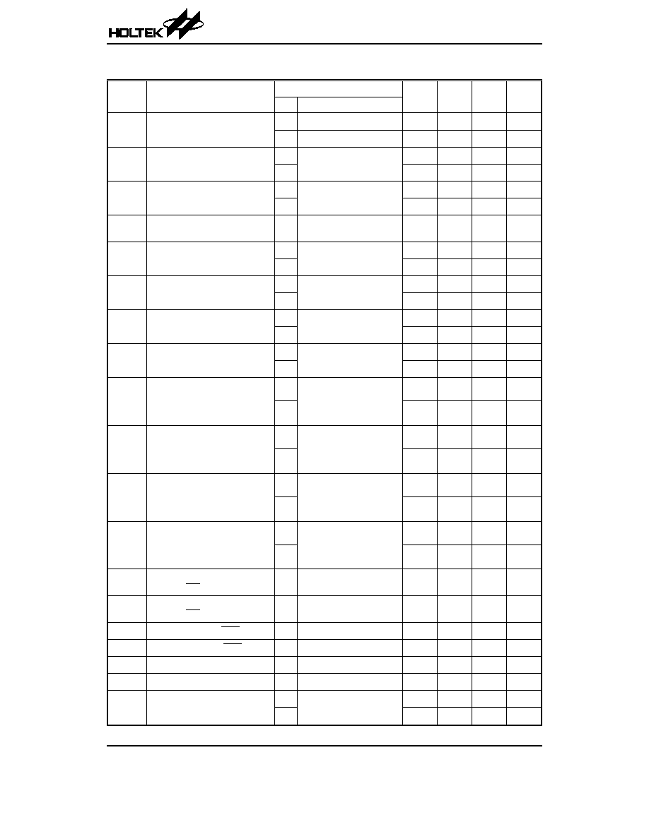
D.C. Characteristics
Ta=25
°C
Symbol
Parameter
Test Conditions
Min.
Typ.
Max.
Unit
V
DD
Conditions
V
DD
Operating Voltage
¾ f
SYS
=4MHz
2.2
¾
5.5
V
¾ f
SYS
=8MHz
3.3
¾
5.5
V
I
DD1
Operating Current
(Crystal OSC)
3V
No load, ADC off
f
SYS
=4MHz
¾
1
2
mA
5V
¾
3
5
mA
I
DD2
Operating Current
(RC OSC)
3V
No load, ADC off
f
SYS
=4MHz
¾
1
2
mA
5V
¾
3
5
mA
I
DD3
Operating Current
(Crystal OSC, RC OSC)
5V
No load, ADC off
f
SYS
=8MHz
¾
4
8
mA
I
DD4
Operating Current
(f
SYS
=32768Hz)
3V
No load, ADC off
¾
0.3
0.6
mA
5V
¾
0.6
1
mA
I
STB1
Standby Current
(*f
S
=T1)
3V
No load, system HALT
LCD off at HALT
¾
¾
1
mA
5V
¾
¾
2
mA
I
STB2
Standby Current
(*f
S
=32.768kHz OSC)
3V
No load, system HALT
LCD on at HALT, C type
¾
2.5
5
mA
5V
¾
10
20
mA
I
STB3
Standby Current
(*f
S
=WDT RC OSC)
3V
No load, system HALT
LCD on at HALT, C type
¾
2
5
mA
5V
¾
6
10
mA
I
STB4
Standby Current
(*f
S
=32.768kHz OSC)
3V
No load, system HALT
LCD on at HALT, R type,
1/2 bias, VLCD=VDD
(Low bias current option)
¾
17
30
mA
5V
¾
34
60
mA
I
STB5
Standby Current
(*f
S
=32.768kHz OSC)
3V
No load, system HALT
LCD on at HALT, R type,
1/3 bias, VLCD=VDD
(Low bias current option)
¾
13
25
mA
5V
¾
28
50
mA
I
STB6
Standby Current
(*f
S
=WDT RC OSC)
3V
No load, system HALT
LCD on at HALT, R type,
1/2 bias, VLCD=VDD
(Low bias current option)
¾
14
25
mA
5V
¾
26
50
mA
I
STB7
Standby Current
(*f
S
=WDT RC OSC)
3V
No load, system HALT
LCD on at HALT, R type,
1/3 bias, VLCD=VDD
(Low bias current option)
¾
10
20
mA
5V
¾
19
40
mA
V
IL1
Input Low Voltage for I/O Ports,
TMR and INT
¾
¾
0
¾
0.3V
DD
V
V
IH1
Input High Voltage for I/O Ports,
TMR and INT
¾
¾
0.7V
DD
¾
V
DD
V
V
IL2
Input Low Voltage (RES)
¾
¾
0
¾
0.4V
DD
V
V
IH2
Input High Voltage (RES)
¾
¾
0.9V
DD
¾
V
DD
V
V
LVR
Low Voltage Reset Voltage
¾
¾
2.7
3.0
3.3
V
V
LVD
Low Voltage Detector Voltage
¾
¾
3.0
3.3
3.6
V
I
OL
I/O Port Segment Logic Output
Sink Current
3V
V
OL
=0.1V
DD
6
12
¾
mA
5V
10
25
¾
mA
HT46R64/HT46C64
Rev. 1.40
5
September 21, 2004
Document Outline
- þÿ
- þÿ
- þÿ
- þÿ
- þÿ
- þÿ
- þÿ
- þÿ
- þÿ
- þÿ
- þÿ
- þÿ
- þÿ