 | –≠–ª–µ–∫—Ç—Ä–æ–Ω–Ω—ã–π –∫–æ–º–ø–æ–Ω–µ–Ω—Ç: HT48CA0 | –°–∫–∞—á–∞—Ç—å:  PDF PDF  ZIP ZIP |
HT48CA0
8-bit Microcontroller
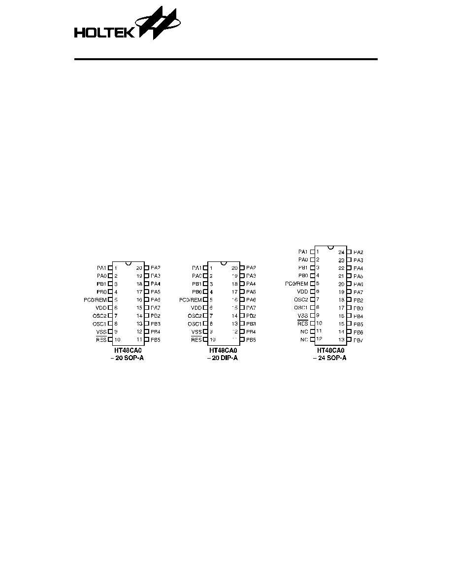
Pin Assignment
Features
∑
Operating voltage: 2.2V~3.6V
∑
Ten bidirectional I/O lines
∑
Six schmitt trigger input lines
∑
One carrier output (1/2 or 1/3 duty)
∑
On-chip crystal and RC oscillator
∑
Watchdog timer
∑
1K
◊
14 program ROM
∑
32
◊
8 data RAM
∑
Low voltage reset function
∑
Halt function and wake-up feature reduce
power consumption
∑
62 powerful instructions
∑
Up to 1
µ
s instruction cycle with 4MHz
system clock
∑
All instructions in 1 or 2 machine cycles
∑
14-bit table read instructions
∑
One-level subroutine nesting
∑
Bit manipulation instructions
General Description
The HT48CA0 is an 8-bit high performance
RISC-like microcontroller specifically designed
for multiple I/O product applications. The de-
vice is particularly suitable for use in products
such as remote controllers, fan/light control-
lers, washing machine controllers, scales, toys
and various subsystem controllers. A halt fea-
ture is included to reduce power consumption.
1
23rd July '98
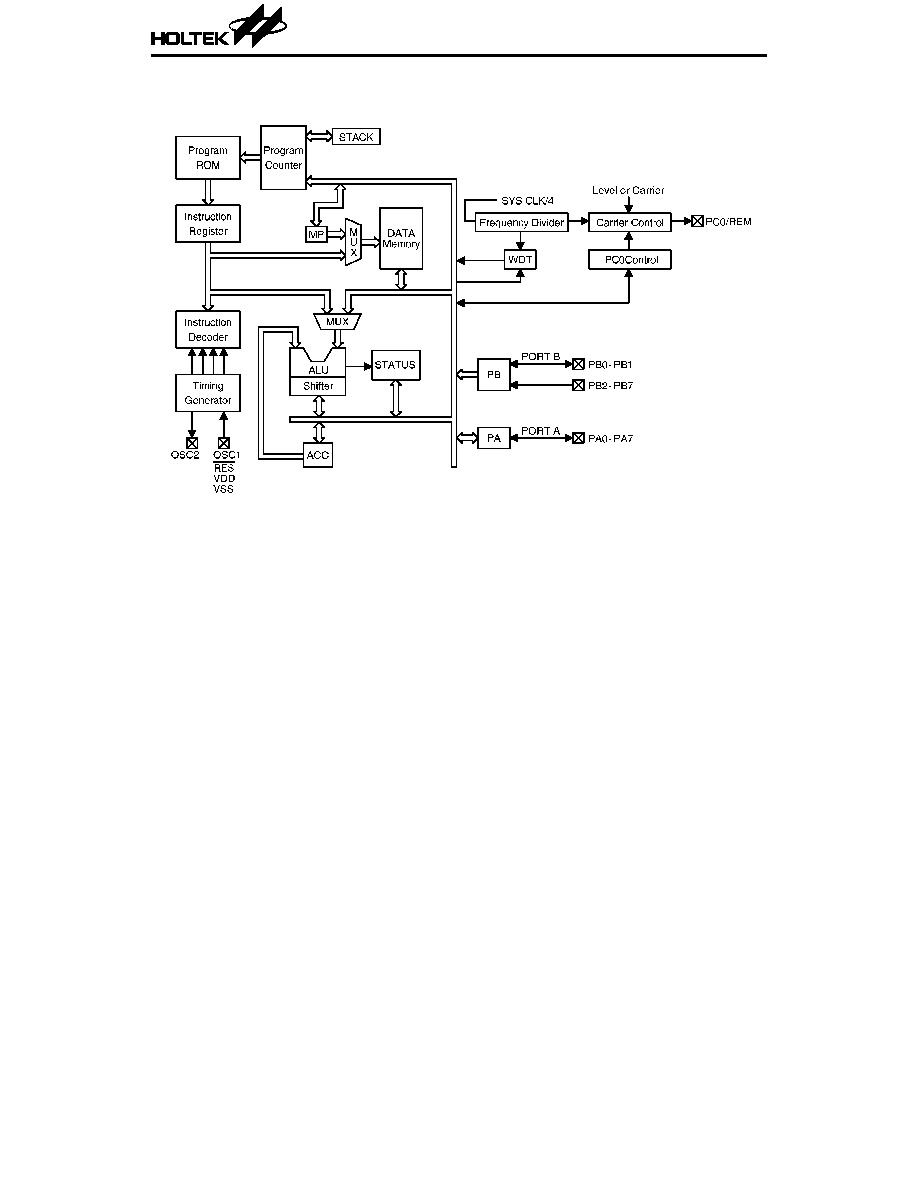
Block Diagram
HT48CA0
2
23rd July '98
Pad Description
Pad No.
Pad Name
I/O
Mask
Option
Function
1, 22
PB0, PB1
I/O
Wake-up
or None
2-bit bidirectional input/output lines with pull-high
resistors. Each bit can be determined as NMOS output
or schmitt trigger input by software instructions. Each
bit can also be configured as wake-up input by mask
option.
2
PC0/REM
O
Level or
Carrier
Level or carrier output pin
PC0 can be set as CMOS output pin or carrier output
pin by mask option.
3
VDD
--
--
Positive power supply
6
VSS
--
--
Negative power supply, GND
7
RES
I
--
Schmitt trigger reset input. Active low.
13~8
PB2~PB7
I
Wake-up
or None
6-bit schmitt trigger input lines with pull-high
resistors. Each bit can be configured as a wake-up
input by mask option.
21~14
PA0~PA7
I/O
--
Bidirectional 8-bit input/output port with pull-high
resistors. Each bit can be determined as NMOS output
or schmitt trigger input by software instructions.
OSC1
OSC2
I
O
Crystal or
RC
OSC1, OSC2 are connected to an RC network or a
crystal (determined by mask option) for the internal
system clock. In the case of RC operation, OSC2 is the
output terminal for 1/4 system clock (NMOS open
drain output).
HT48CA0
3
23rd July '98

Pad Assignment
* The IC substrate should be connected to VSS in the PCB layout artwork.
* The TMR pad must be bonded to VDD or VSS if the TMR pad is not used.
Absolute Maximum Ratings*
Supply Voltage ................................. ≠0.3V to 4V
Storage Temperature................. ≠50
∞
C to 125
∞
C
Input Voltage................. V
SS
≠0.3V to V
DD
+0.3V
Operating Temperature............... ≠25
∞
C to 70
∞
C
*Note: These are stress ratings only. Stresses exceeding the range specified under "Absolute Maxi-
mum Ratings" may cause substantial damage to the device. Functional operation of this
device at other conditions beyond those listed in the specification is not implied and prolonged
exposure to extreme conditions may affect device reliability.
HT48CA0
4
23rd July '98
D.C. Characteristics
Ta=25
∞
C
Symbol
Parameter
Test Conditions
Min.
Typ.
Max. Unit
V
DD
Conditions
V
DD
Operating Voltage
--
--
2.2
--
3.6
V
I
DD
Operating Current
3V
No load,
f
SYS
=4MHz
--
0.7
1.5
mA
I
STB
Standby Current
3V
No load,
system HALT
--
--
1
µ
A
V
IL1
Input Low Voltage for I/O Ports
3V
--
0
--
1.05
V
V
IH1
Input High Voltage for I/O Ports
3V
--
1.95
--
3
V
V
IL2
Input Low Voltage (RES)
3V
--
--
1.5
--
V
V
IH2
Input High Voltage (RES)
3V
--
--
2.4
--
V
I
OL
I/O Ports Sink Current
3V
V
OL
=0.3V
1.5
2.5
--
mA
I
OH
I/O Ports Source Current
3V
V
OH
=2.7V
≠1
≠1.5
--
mA
R
PH1
Pull-high Resistance of PA
Port, PB0~PB1 and RES
3V
--
--
60
--
k
R
PH2
Pull-high Resistance of PB2~PB7
3V
--
--
60
--
k
V
LVR
Low Voltage Reset
3V
--
1.8
2.0
2.2
V
A.C. Characteristics
Ta=25
∞
C
Symbol
Parameter
Test Conditions
Min.
Typ. Max. Unit
V
DD
Conditions
f
SYS
System Clock
3V
--
400
--
4000
kHz
t
RES
External Reset Low Pulse Width
--
--
1
--
--
µ
s
t
SST
System Start-up timer
Period
--
Power-up or
wake-up from halt
--
1024
--
t
SYS
Note: t
SYS
=1/f
SYS
HT48CA0
5
23rd July '98