 | –≠–ª–µ–∫—Ç—Ä–æ–Ω–Ω—ã–π –∫–æ–º–ø–æ–Ω–µ–Ω—Ç: HT48CA5 | –°–∫–∞—á–∞—Ç—å:  PDF PDF  ZIP ZIP |
Document Outline
- ˛ˇ
- ˛ˇ
- ˛ˇ
- ˛ˇ
- ˛ˇ
- ˛ˇ
- ˛ˇ
- ˛ˇ
- ˛ˇ
- ˛ˇ
- ˛ˇ
- ˛ˇ
- ˛ˇ
- ˛ˇ
- ˛ˇ

HT48RA5/HT48CA5
Remote Type 8-Bit MCU
Rev. 1.20
1
June 10, 2005
General Description
The HT48RA5/HT48CA5 are 8-bit high performance,
RISC architecture microcontroller devices specifically
designed for multiple I/O control product applications.
The data ROM can be used to store remote control
codes. The mask version HT48CA5 is fully pin and func-
tionally compatible with the OTP version HT48RA5 de-
vice.
The advantages of low power consumption, I/O flexibil-
ity, timer functions, oscillator options, watchdog timer,
programmable frequency divider, HALT and wake-up
functions, as well as low cost, enhance the versatility of
these devices to suit a wide range of application possi-
bilities such as industrial control, consumer products,
subsystem controllers, and particularly suitable for use
in products such as universal remote controller (URC).
Features
∑
Operating voltage: 2.0V~5.5V
∑
23 bidirectional I/O lines (max.)
∑
1 interrupt input shared with an I/O line
∑
8-bit programmable timer/event counter with
overflow interrupt and 8-stage prescaler (TMR0)
∑
16-bit programmable timer/event counter and
overflow interrupts (TMR1)
∑
On-chip crystal and RC oscillator
∑
Watchdog Timer
∑
40K
¥16 program memory (8K¥16 bits¥5 banks)
∑
224
¥8 data memory RAM
∑
PFD supported
∑
HALT function and wake-up feature reduce power
consumption
∑
8-level subroutine nesting
∑
Up to 1
ms instruction cycle with 4MHz system clock at
V
DD
=3V
∑
Bit manipulation instruction
∑
16-bit table read instruction
∑
63 powerful instructions
∑
All instructions in one or two machine cycles
∑
Low voltage reset function
∑
28-pin SOP/SSOP (209mil) package
Technical Document
∑
Tools Information
∑
FAQs
∑
Application Note
-
HA0016E Writing and Reading to the HT24 EEPROM with the HT48 MCU Series
-
HA0018E Controlling the HT1621 LCD Controller with the HT48 MCU Series
-
HA0041E Using the HT48CA0 to Generate the HT6221 Output Signals
-
HA0075E MCU Reset and Oscillator Circuits Application Note
-
HA0076E HT48RAx/HT48CAx Software Application Note
-
HA0082E HT48xA0-1 and HT48xA0-2 Power-on Reset Timing

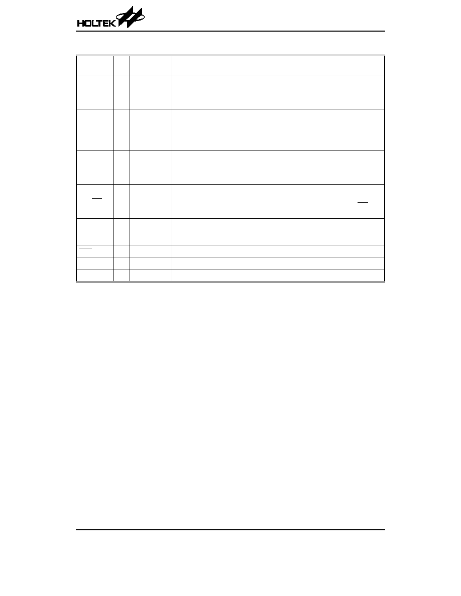
Block Diagram
Pin Assignment
HT48RA5/HT48CA5
Rev. 1.20
2
June 10, 2005
2 8
2 7
2 6
2 5
2 4
2 3
2 2
2 1
2 0
1 9
1 8
1 7
1 6
1 5
1
2
3
4
5
6
7
8
9
1 0
1 1
1 2
1 3
1 4
P B 6
P B 7
P A 4
P A 5
P A 6
P A 7
O S C 2
O S C 1
V D D
R E S
P C 5 / T M R 1
P C 4
P C 3
P C 2
P B 5
P B 4
P A 3
P A 2
P A 1
P A 0
P B 3
P B 2
P B 1
P B 0 / P F D
V S S
P F 0 / I N T
P C 0 / T M R 0
P C 1
H T 4 8 R A 5 / H T 4 8 C A 5
2 8 S O P - A / S S O P - A
P F 0 / I N T
O S C 2
O S C 1
R E S
V D D
M U X
P C 0 / T M R 0
T M R 0 C
T M R 0
V S S
P r e s c a l e r
f
S Y S
P r o g r a m
R O M
P r o g r a m
C o u n t e r
I n t e r r u p t
C i r c u i t
S T A C K
I N T C
D A T A
M e m o r y
I n s t r u c t i o n
R e g i s t e r
M
U
X
I n s t r u c t i o n
D e c o d e r
S T A T U S
A L U
S h i f t e r
T i m i n g
G e n e r a t o r
A C C
M
U
X
M P
W D T S
W D T
W D T O S C
W D T P r e s c a l e r
M
U
X
E N / D I S
P F C
P F
P O R T F
P F 0 / I N T
P B C
P O R T B
P B 0 / P F D
P B 1 ~ P B 7
P F D
P B
P A C
P O R T A
P A 0 ~ P A 7
P A
P C
P O R T C
P C 0 / T M R 0
P C 1 ~ P C 4
P C 5 / T M R 1
P C C
T M R 1 C
T M R 1
M
U
X
P C 5 / T M R 1
f
S Y S
/ 4
f
S Y S
/ 4
B P
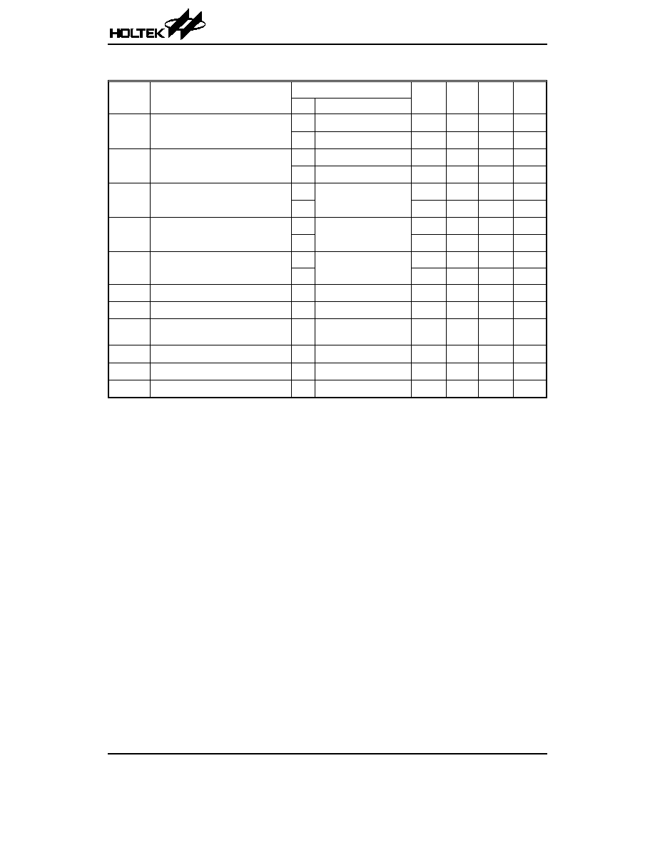
Pin Description
Pin Name
I/O
ROM Code
Option
Description
PA0~PA7
I/O
Wake-up*
Pull-high***
Bidirectional 8-bit input/output port. Each bit can be configured as a wake-up in-
put by a option. Software instructions determine the CMOS output or Schmitt trig-
ger input with/without pull-high resistor. The pull-high resistor of each input/output
line is also optional.
PB0/PFD
PB1~PB7
I/O
Pull-high**
PB0 or PFD
Bidirectional 8-bit input/output port. Software instructions determine the CMOS
output or Schmitt trigger input with/without pull-high resistor. The pull-high resis-
tor of each input/output line is also optional. The output mode of PB0 can be
used as an internal PFD signal output and it can be used as a various frequency
carrier signal.
PC0/TMR0
PC1~PC4
PC5/TMR1
I/O
Pull-high*
Bidirectional 6-bit input/output port. Software instructions determine the CMOS
output or Schmitt trigger input with/without pull-high resistor. The pull-high resis-
tor of each input/output line is also optional. PC0 and PC5 are pin shared with
TMR0 and TMR1 function pins.
PF0/INT
I/O
Pull-high*
Bidirectional 1-bit input/output port. Software instructions determine the CMOS
output or Schmitt trigger input with/without pull-high resistor. The pull-high resis-
tor of this input/output line is also optional. PF0 is pin shared with the INT func-
tion pin.
OSC1
OSC2
I
O
Crystal
or RC
OSC1, OSC2 are connected to an RC network or Crystal (determined by option)
for the internal system clock. In the case of RC operation, OSC2 is the output
terminal for 1/4 system clock.
RES
I
æ
Schmitt trigger reset input, active low.
VSS
æ
æ
Negative power supply, ground
VDD
æ
æ
Positive power supply
Note:
* Bit option
** Nibble option
*** Byte option
Absolute Maximum Ratings
Supply Voltage ...........................V
SS
-0.3V to V
SS
+6.0V
Storage Temperature ............................
-50∞C to 125∞C
Input Voltage..............................V
SS
-0.3V to V
DD
+0.3V
Operating Temperature...........................
-40∞C to 85∞C
Note: These are stress ratings only. Stresses exceeding the range specified under
≤Absolute Maximum Ratings≤ may
cause substantial damage to the device. Functional operation of this device at other conditions beyond those
listed in the specification is not implied and prolonged exposure to extreme conditions may affect device reliabil-
ity.
HT48RA5/HT48CA5
Rev. 1.20
3
June 10, 2005

D.C. Characteristics
Ta=25
∞C
Symbol
Parameter
Test Conditions
Min.
Typ.
Max.
Unit
V
DD
Conditions
V
DD
Operating Voltage
æ
æ
2.0
æ
5.5
V
I
DD1
Operating Current
3V
No load, f
SYS
=4MHz
æ
0.6
1.5
mA
5V
æ
2
4
mA
I
DD2
Operating Current
(Crystal OSC, RC OSC)
5V
No load, f
SYS
=8MHz
æ
4
8
mA
I
STB1
Standby Current (WDT Enabled and
WDT RC OSC On)
3V
No load, system HALT
æ
1.1
5
mA
5V
æ
4
10
mA
I
STB2
Standby Current (WDT Disabled)
3V
No load, system HALT
æ
0.1
1
mA
5V
æ
0.2
2
mA
V
IL1
Input Low Voltage for I/O Ports
æ
æ
0
æ
0.3V
DD
V
V
IH1
Input High Voltage for I/O Ports
æ
æ
0.7V
DD
æ
V
DD
V
V
IL2
Input Low Voltage (RES)
æ
æ
0
æ
0.4V
DD
V
V
IH2
Input High Voltage (RES)
æ
æ
0.9V
DD
æ
V
DD
V
V
LVR
Low Voltage Reset
æ
LVR=2.0V
1.8
1.9
2.0
V
LVR=3.0V
2.7
3.0
3.3
V
I
OL
I/O Port Sink Current
3V
V
OL
=0.1V
DD
4
8
æ
mA
5V
10
20
æ
mA
I
OH
I/O Port Source Current
3V
V
OH
=0.9V
DD
-2
-4
æ
mA
5V
-5
-10
æ
mA
R
PH
Pull-high Resistance
3V
æ
20
60
100
k
W
5V
10
30
50
k
W
HT48RA5/HT48CA5
Rev. 1.20
4
June 10, 2005
A.C. Characteristics
Ta=25
∞C
Symbol
Parameter
Test Conditions
Min.
Typ.
Max.
Unit
V
DD
Conditions
f
SYS1
System Clock (Crystal OSC)
æ
2.0V~5.5V
400
æ
4000
kHz
æ
3.3V~5.5V
400
æ
8000
kHz
f
SYS2
System Clock (RC OSC)
æ
2.0V~5.5V
400
æ
4000
kHz
æ
3.3V~5.5V
400
æ
8000
kHz
f
TIMER
Timer I/P Frequency (TMR0/TMR1)
3V
50% duty
0
æ
4000
kHz
5V
0
æ
8000
kHz
t
WDTOSC
Watchdog Oscillator Period
3V
æ
45
90
180
ms
5V
32
65
130
ms
t
WDT1
Watchdog Time-out Period
(WDT OSC)
3V
Without WDT prescaler
11
23
46
ms
5V
8
17
33
ms
t
WDT2
Watchdog Time-out Period (f
SYS
/4)
æ
Without WDT prescaler
æ
1024
æ
t
SYS
t
RES
External Reset Low Pulse Width
æ
æ
1
æ
æ
ms
t
SST
System Start-up Timer Period
æ
Power-up reset or
wake-up from HALT
æ
1024
æ
t
SYS
t
LVR
Low Voltage Width to Reset
æ
æ
1
æ
æ
ms
t
INT
Interrupt Pulse Width
æ
æ
1
æ
æ
ms
t
ACC
Data ROM Access Time
æ
æ
1
æ
æ
ms
Note: t
SYS
=1/(f
SYS
)
HT48RA5/HT48CA5
Rev. 1.20
5
June 10, 2005