Äîêóìåíòàöèÿ è îïèñàíèÿ www.docs.chipfind.ru

HT48R70A-1/HT48C70-1
I/O Type 8-Bit MCU
Rev. 1.60
1
June 9, 2004
General Description
The HT48R70A-1/HT48C70-1 are 8-bit high perfor-
mance, RISC architecture microcontroller devices spe-
cifically designed for multiple I/O control product
applications. The mask version HT48C70-1 is fully pin
and functionally compatible with the OTP version
HT48R70A-1 device.
The advantages of low power consumption, I/O flexibil-
ity, timer functions, oscillator options, HALT and
wake-up functions, watchdog timer, buzzer driver, as
well as low cost, enhance the versatility of these devices
to suit a wide range of application possibilities such as
industrial control, consumer products, subsystem con-
trollers, etc.
Features
·
Operating voltage:
f
SYS
=4MHz: 2.2V~5.5V
f
SYS
=8MHz: 3.3V~5.5V
·
Low voltage reset function
·
56 bidirectional I/O lines (max.)
·
1 interrupt input
·
2
´16-bit programmable timer/event counter and
overflow interrupts
·
On-chip RC oscillator, external crystal and RC oscil-
lator
·
32768Hz crystal oscillator for timing purposes only
·
Watchdog Timer
·
8192
´16 program memory ROM
·
224
´8 data memory RAM
·
HALT function and wake-up feature reduce power
consumption
·
16-level subroutine nesting
·
Up to 0.5
ms instruction cycle with 8MHz system clock
at V
DD
=5V
·
Bit manipulation instruction
·
16-bit table read instruction
·
63 powerful instructions
·
All instructions in one or two machine cycles
·
48-pin SSOP, 64-pin QFP package
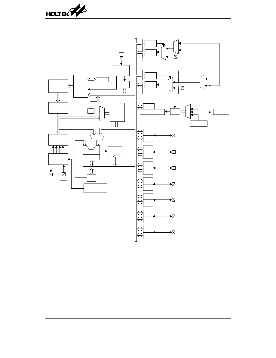
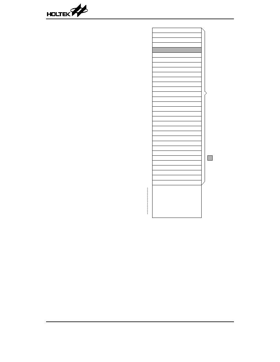
Block Diagram
HT48R70A-1/HT48C70-1
Rev. 1.60
2
June 9, 2004
I N T
O S C 2
O S C 1
R E S
V D D
M U X
T M R 0 C
V S S
P r o g r a m
R O M
P r o g r a m
C o u n t e r
I n t e r r u p t
C i r c u i t
S T A C K
I N T C
D A T A
M e m o r y
I n s t r u c t i o n
R e g i s t e r
M
U
X
I n s t r u c t i o n
D e c o d e r
S T A T U S
A L U
S h i f t e r
T i m i n g
G e n e r a t o r
A C C
M P
W D T S
W D T
W D T O S C
W D T P r e s c a l e r
M
U
X
R T C O S C
E N / D I S
I n t e r n a l
R C O S C
P D C
P O R T D
P D 0 ~ P D 7
P G C
P G
P O R T G
P G 0 ~ P G 7
P B C
P O R T B
P B 0 ~ P B 7
P B
P A C
P O R T A
P A 0 ~ P A 7
P A
P D
P C
P O R T C
P C 0 ~ P C 7
P C C
T M R 1 C
T M R 1 L
T M R 1 H
M
U
X
M
U
X
T M R 1
f
S Y S
/ 4
T M R 0
T M R 0 L
T M R 0 H
M
U
X
M
U
X
f
S Y S
/ 4
P E C
P O R T E
P E 0 ~ P E 7
P F C
P F
P O R T F
P F 0 ~ P F 7
P E
f
S Y S
/ 4
Pin Assignment
HT48R70A-1/HT48C70-1
Rev. 1.60
3
June 9, 2004
P B 6
P B 7
P A 4
P A 5
P A 6
P A 7
P F 0
P F 1
P F 2
P F 3
O S C 2
O S C 1
V D D
R E S
T M R 1
P D 3
P D 2
P D 1
P D 0
P C 7
P C 6
P C 5
P C 4
P C 3
P B 5
P B 4
P A 3
P A 2
P A 1
P A 0
P B 3
P B 2
P B 1
P B 0
P E 3
P E 2
P E 1
P E 0
P D 7
P D 6
P D 5
P D 4
V S S
I N T
T M R 0
P C 0
P C 1
P C 2
P
A
6
P
A
5
P
A
4
P
B
7
P
B
6
P
B
5
P
B
4
P
G
7
P
G
6
P
G
5
P
G
4
P
A
3
P
A
2
P A 7
P F 0
P F 1
P F 2
P F 3
O S C 2
O S C 1
P F 4
P F 5
P F 6
P F 7
V D D
R E S
T M R 1
P D 3
P D 2
P D 1
P D 0
P C 7
2 0 2 1 2 2 2 3 2 4
P A 1
P A 0
P E 7
P E 6
P E 5
P E 4
P B 3
P B 2
P B 1
P B 0
P E 3
P E 2
P E 1
P E 0
P D 7
P D 6
P D 5
P D 4
V S S
P
C
6
P
C
5
P
C
4
P
C
3
P
C
2
P
C
1
P
C
0
P
G
3
P
G
2
P
G
1
P
G
0
T
M
R
0
I
N
T
3 2
3 1
3 0
2 9
2 8
2 7
2 6
2 5
1
2
3
4
5
6
7
8
9
1 0
1 1
1 2
1 3
1 4
1 5
1 6
1 7
1 8
1 9
5 1
5 0
4 9
4 8
4 7
4 6
4 5
4 4
4 3
4 2
4 1
4 0
3 9
3 8
3 7
3 6
3 5
3 4
3 3
6 4 6 3 6 2 6 1 6 0
5 2
5 3
5 4
5 5
5 6
5 7
5 8
5 9
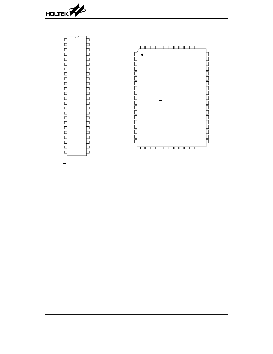
H T 4 8 R 7 0 A - 1 / H T 4 8 C 7 0 - 1
4 8 S S O P - A
H T 4 8 R 7 0 A - 1 / H T 4 8 C 7 0 - 1
6 4 Q F P - A
4 8
4 7
4 6
4 5
4 4
4 3
4 2
4 1
4 0
3 9
3 8
3 7
3 6
3 5
3 4
3 3
3 2
3 1
3 0
2 9
2 8
2 7
2 6
2 5
1
2
3
4
5
6
7
8
9
1 0
1 1
1 2
1 3
1 4
1 5
1 6
1 7
1 8
1 9
2 0
2 1
2 2
2 3
2 4
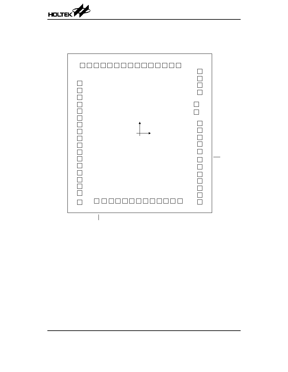
Pad Assignment
HT48C70-1
* The IC substrate should be connected to VSS in the PCB layout artwork.
HT48R70A-1/HT48C70-1
Rev. 1.60
4
June 9, 2004
6 4
6 3
6 2
6 1
6 0
5 9
5 8
5 7
5 6
5 5
5 4
5 3
5 2
5 1
5 0
4 9
4 8
4 7
4 6
4 5
1
2
3
4
5
6
7
8
9
1 0
1 1
1 2
1 3
1 4
1 5
1 6
1 7
1 8
1 9
2 0
2 1
2 2
2 3
2 4
2 5
2 6
2 7
2 8
2 9
3 0
3 1
3 2
3 3
3 4
3 5
3 6
3 7
3 8
3 9
4 0
4 4
4 3
4 2
4 1
( 0 , 0 )
P A 1
P A 0
P E 7
P E 6
P E 5
P E 4
P B 3
P B 2
P B 1
P B 0
P E 3
P E 2
P E 1
P E 0
P D 7
P D 6
P D 5
P D 4
V S S
P
C
6
P
C
5
P
C
4
P
C
3
P
C
2
P
C
1
P
C
0
P
G
3
P
G
2
P
G
1
P
G
0
T
M
R
0
I
N
T
P F 0
P F 1
P F 2
P F 3
O S C 2
O S C 1
P F 4
P F 5
P F 6
P F 7
V D D
R E S
T M R 1
P D 3
P D 2
P D 1
P D 0
P C 7
P
A
7
P
A
6
P
A
5
P
A
4
P
B
7
P
B
6
P
B
5
P
B
4
P
G
7
P
G
6
P
G
5
P
G
4
P
A
3
P
A
2
Pad Description
Pad Name
I/O
Options
Description
PA0~PA7
I/O
Wake-up
Pull-high*
CMOS or Schmitt
Input
Bidirectional 8-bit input/output ports
Each bit can be configured as a wake-up input by options. Software instruc-
tions determine the CMOS output or Schmitt trigger or CMOS input with or with-
out pull high resistor (by options).
PB0~PB7
I/O
Pull-high*
Bidirectional 8-bit input/output ports
Software instructions determine the CMOS output or Schmitt trigger input
(pull-high depends on options).
VSS
¾
¾
Negative power supply, ground
INT
I
¾
External interrupt Schmitt trigger without pull high resistor
Edge trigger is activated during high to low transition.
TMR0
I
¾
Schmitt trigger input for Timer/Event Counter 0
TMR1
I
¾
Schmitt trigger input for Timer/Event Counter 1
PC0~PC7
I/O
Pull-high*
Bidirectional 8-bit input/output ports
Software instructions determine the CMOS output or Schmitt trigger input
(pull-high depends on options).
RES
I
¾
Schmitt trigger reset input, active low
VDD
¾
¾
Positive power supply
OSC1
OSC2
I
O
Crystal
or RC
or RTC
OSC1 and OSC2 are connected to an RC network or a crystal (by options) for
the internal system clock. In the case of RC operation, OSC2 is the output
terminal for 1/4 system clock.
These two pins also can be optioned as an RTC oscillator (32768Hz). In this
case, the system clock comes from an internal RC oscillator whose fre-
quency has 4 options (3.2MHz, 1.6MHz, 800kHz, 400kHz)
PD0~PD7
I/O
Pull-high*
Bidirectional 8-bit input/output ports
Software instructions determine the CMOS output or Schmitt trigger input
(pull-high depends on options).
PE0~PE7
I/O
Pull-high*
Bidirectional 8-bit input/output ports
Software instructions determine the CMOS output or Schmitt trigger input
(pull-high depends on options).
PF0~PF7
I/O
Pull-high*
Bidirectional 8-bit input/output ports
Software instructions determine the CMOS output or Schmitt trigger input
(pull-high depends on options).
PG0~PG7
I/O
Pull-high*
Bidirectional 8-bit input/output ports
Software instructions determine the CMOS output or Schmitt trigger input
(pull-high depends on options).
Note:
* The pull-high resistors of each I/O port (PA, PB, PC, PD, PE, PF, PG) are controlled by an option.
CMOS or Schmitt trigger option of port A is controlled by an option.
Absolute Maximum Ratings
Supply Voltage ...........................V
SS
-0.3V to V
SS
+6.0V
Storage Temperature ............................
-50°C to 125°C
Input Voltage..............................V
SS
-0.3V to V
DD
+0.3V
Operating Temperature...........................
-40°C to 85°C
Note: These are stress ratings only. Stresses exceeding the range specified under
²Absolute Maximum Ratings² may
cause substantial damage to the device. Functional operation of this device at other conditions beyond those
listed in the specification is not implied and prolonged exposure to extreme conditions may affect device reliabil-
ity.
HT48R70A-1/HT48C70-1
Rev. 1.60
5
June 9, 2004
D.C. Characteristics
Ta=25
°C
Symbol
Parameter
Test Conditions
Min.
Typ.
Max.
Unit
V
DD
Conditions
V
DD
Operating Voltage
¾ f
SYS
=4MHz
2.2
¾
5.5
V
¾ f
SYS
=8MHz
3.3
¾
5.5
V
I
DD1
Operating Current (Crystal OSC)
3V
No load, f
SYS
=4MHz
¾
0.6
1.5
mA
5V
¾
2
4
mA
I
DD2
Operating Current (RC OSC)
3V
No load, f
SYS
=4MHz
¾
0.8
1.5
mA
5V
¾
2.5
4
mA
I
DD3
Operating Current (Crystal OSC)
5V No load, f
SYS
=8MHz
¾
3
5
mA
I
STB1
Standby Current (WDT Enabled RTC Off)
3V
No load, system HALT
¾
¾
5
mA
5V
¾
¾
10
mA
I
STB2
Standby Current (WDT Disabled RTC Off)
3V
No load, system HALT
¾
¾
1
mA
5V
¾
¾
2
mA
I
STB3
Standby Current (WDT Disabled, RTC On)
3V
No load, system HALT
¾
¾
5
mA
5V
¾
¾
10
mA
V
IL1
Input Low Voltage for I/O Ports
¾
¾
0
¾
0.3V
DD
V
V
IH1
Input High Voltage for I/O Ports
¾
¾
0.7V
DD
¾
V
DD
V
V
IL2
Input Low Voltage (RES)
¾
¾
0
¾
0.4V
DD
V
V
IH2
Input High Voltage (RES)
¾
¾
0.9V
DD
¾
V
DD
V
V
LVR
Low Voltage Reset
¾ LVRenabled
2.7
3.0
3.3
V
I
OL
I/O Port Sink Current
3V V
OL
=0.1V
DD
4
8
¾
mA
5V V
OL
=0.1V
DD
10
20
¾
mA
I
OH
I/O Port Source Current
3V V
OH
=0.9V
DD
-2
-4
¾
mA
5V V
OH
=0.9V
DD
-5
-10
¾
mA
R
PH
Pull-high Resistance
3V
¾
20
60
100
k
W
5V
10
30
50
k
W
HT48R70A-1/HT48C70-1
Rev. 1.60
6
June 9, 2004
A.C. Characteristics
Ta=25
°C
Symbol
Parameter
Test Conditions
Min.
Typ.
Max.
Unit
V
DD
Conditions
f
SYS1
System Clock (Crystal OSC)
¾ 2.2V~5.5V
400
¾
4000
kHz
¾ 3.3V~5.5V
400
¾
8000
kHz
f
SYS2
System Clock (RC OSC)
¾ 2.2V~5.5V
400
¾
4000
kHz
¾ 3.3V~5.5V
400
¾
8000
kHz
f
SYS3
System Clock (Internal RC OSC)
5V
3.2MHz
1800
¾
5400
kHz
1.6MHz
900
¾
2700
kHz
800kHz
450
¾
1350
kHz
400kHz
225
¾
675
kHz
f
TIMER
Timer I/P Frequency (TMR)
¾ 2.2V~5.5V
0
¾
4000
kHz
¾ 3.3V~5.5V
0
¾
8000
kHz
t
WDTOSC
Watchdog Oscillator Period
3V
¾
45
90
180
ms
5V
¾
32
65
130
ms
t
WDT1
Watchdog Time-out Period (WDT OSC)
3V
Without WDT prescaler
11
23
46
ms
5V
8
17
33
ms
t
WDT2
Watchdog Time-out Period (System Clock)
¾ Without WDT prescaler
¾
1024
¾
t
SYS
t
WDT3
Watchdog Time-out Period (RTC OSC)
¾ Without WDT prescaler
¾
7.812
¾
ms
t
RES
External Reset Low Pulse Width
¾
¾
1
¾
¾
ms
t
SST
System Start-up Timer Period
¾ Wake-up from HALT
¾
1024
¾
t
SYS
t
INT
Interrupt Pulse Width
¾
¾
1
¾
¾
ms
HT48R70A-1/HT48C70-1
Rev. 1.60
7
June 9, 2004
Functional Description
HT48R70A-1/HT48C70-1
Rev. 1.60
8
June 9, 2004
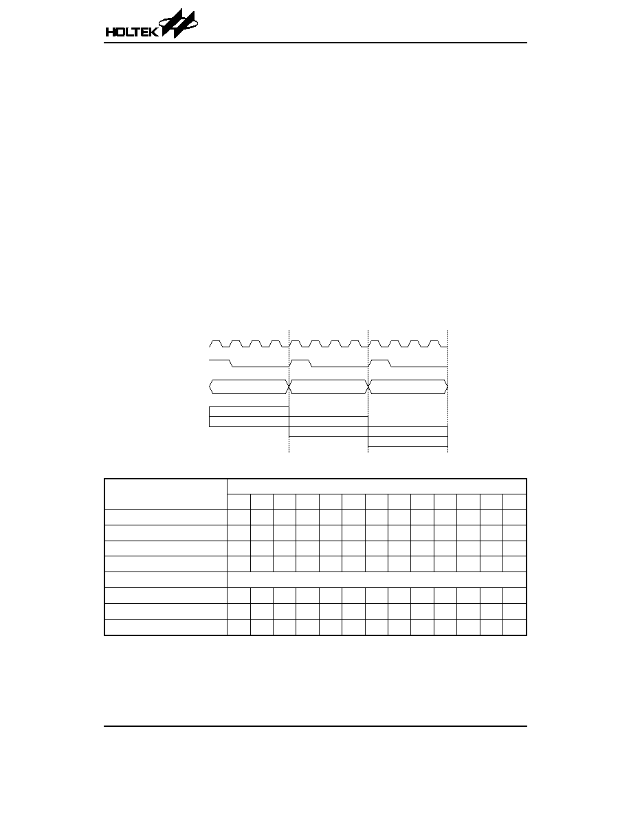
Execution Flow
The system clock for the microcontroller is derived from
either a crystal or an RC oscillator. The system clock is
internally divided into four non-overlapping clocks. One
instruction cycle consists of four system clock cycles.
Instruction fetching and execution are pipelined in such
a way that a fetch takes an instruction cycle while de-
coding and execution takes the next instruction cycle.
However, the pipelining scheme causes each instruc-
tion to effectively execute in a cycle. If an instruction
changes the program counter, two cycles are required to
complete the instruction.
Program Counter
- PC
The program counter (PC) controls the sequence in
which the instructions stored in the program ROM are
executed and its contents specify a full range of pro-
gram memory.
After accessing a program memory word to fetch an in-
struction code, the contents of the program counter are
incremented by one. The program counter then points to
the memory word containing the next instruction code.
When executing a jump instruction, conditional skip ex-
ecution, loading register, subroutine call or return from
subroutine, initial reset, internal interrupt, external inter-
rupt or return from interrupts, the PC manipulates the
program transfer by loading the address corresponding
to each instruction.
The conditional skip is activated by instructions. Once
the condition is met, the next instruction, fetched during
the current instruction execution, is discarded and a
dummy cycle replaces it to get the proper instruction.
Otherwise proceed to the next instruction.
The lower byte of the program counter (PCL) is a read-
able and writeable register (06H). Moving data into the
PCL performs a short jump. The destination will be
within the current program ROM page.
When a control transfer takes place, an additional
dummy cycle is required.
T 1
T 2
T 3
T 4
T 1
T 2
T 3
T 4
T 1
T 2
T 3
T 4
F e t c h I N S T ( P C )
E x e c u t e I N S T ( P C - 1 )
F e t c h I N S T ( P C + 1 )
E x e c u t e I N S T ( P C )
F e t c h I N S T ( P C + 2 )
E x e c u t e I N S T ( P C + 1 )
P C
P C + 1
P C + 2
S y s t e m C l o c k
O S C 2 ( R C o n l y )
P C
Execution Flow
Mode
Program Counter
*12
*11
*10
*9
*8
*7
*6
*5
*4
*3
*2
*1
*0
Initial Reset
0
0
0
0
0
0
0
0
0
0
0
0
0
External Interrupt
0
0
0
0
0
0
0
0
0
0
1
0
0
Timer/Event Counter 0 Overflow
0
0
0
0
0
0
0
0
0
1
0
0
0
Timer/Event Counter 1 Overflow
0
0
0
0
0
0
0
0
0
1
1
0
0
Skip
PC+2
Loading PCL
*12
*11
*10
*9
*8
@7
@6
@5
@4
@3
@2
@1
@0
Jump, Call Branch
#12
#11
#10
#9
#8
#7
#6
#5
#4
#3
#2
#1
#0
Return from Subroutine
S12
S11
S10
S9
S8
S7
S6
S5
S4
S3
S2
S1
S0
Program Counter
Note: *12~*0: Program counter bits
S12~S0: Stack register bits
#12~#0: Instruction code bits
@7~@0: PCL bits
HT48R70A-1/HT48C70-1
Rev. 1.60
9
June 9, 2004
Program Memory
- ROM
The program memory is used to store the program in-
structions which are to be executed. It also contains
data, table, and interrupt entries, and is organized into
8192
´16 bits, addressed by the program counter and ta-
ble pointer.
Certain locations in the program memory are reserved
for special usage:
·
Location 000H
This area is reserved for program initialization. After
chip reset, the program always begins execution at lo-
cation 000H.
·
Location 004H
This area is reserved for the external interrupt service
program. If the INT interrupt pin is activated, the inter-
rupt enabled and the stack is not full, the program be-
gins execution at location 004H.
·
Location 008H
This area is reserved for the Timer/Event Counter 0 in-
terrupt service program. If a timer interrupt results from a
Timer/Event Counter 0 overflow, and if the interrupt is
enabled and the stack is not full, the program begins ex-
ecution at location 008H .
·
Location 00CH
This location is reserved for the Timer/Event Counter
1 interrupt service program. If a timer interrupt results
from a Timer/Event Counter 1 overflow, and the inter-
rupt is enabled and the stack is not full, the program
begins execution at location 00CH.
·
Table location
Any location in the program memory can be used as
look-up tables. The instructions
²TABRDC [m]² (the
current page, one page=256 words) and
²TABRDL
[m]
² (the last page) transfer the contents of the
lower-order byte to the specified data memory, and
the higher-order byte to TBLH (08H). The Table
Higher-order byte register (TBLH) is read only. The ta-
ble pointer (TBLP) is a read/write register (07H),
which indicates the table location. Before accessing
the table, the location must be placed in the TBLP. The
TBLH is read only and cannot be restored. If the main
routine and the ISR (Interrupt Service Routine) both
employ the table read instruction, the contents of the
TBLH in the main routine are likely to be changed by
the table read instruction used in the ISR. Errors can
occur. In other words, using the table read instruction
in the main routine and the ISR simultaneously should
be avoided. However, if the table read instruction has
to be applied in both the main routine and the ISR, the
interrupt is supposed to be disabled prior to the table
read instruction. It will not be enabled until the TBLH
has been backed up. All table related instructions re-
quire two cycles to complete the operation. These ar-
eas may function as normal program memory
depending upon the requirements.
Stack Register
- STACK
This is a special part of the memory which is used to
save the contents of the program counter (PC) only. The
stack is organized into 16 levels and is neither part of the
data nor part of the program space, and is neither read-
able nor writeable. The activated level is indexed by the
stack pointer (SP) and is neither readable nor writeable.
At a subroutine call or interrupt acknowledge signal, the
1 6 b i t s
1 F F F H
n F F H
P r o g r a m
M e m o r y
D e v i c e I n i t i a l i z a t i o n P r o g r a m
E x t e r n a l I n t e r r u p t S u b r o u t i n e
T i m e r / E v e n t C o u n t e r 0
I n t e r r u p t S u b r o u t i n e
L o o k - u p T a b l e ( 2 5 6 w o r d s )
L o o k - u p T a b l e ( 2 5 6 w o r d s )
N o t e : n r a n g e s f r o m 0 t o 1 F
0 0 C H
n 0 0 H
0 0 8 H
0 0 4 H
0 0 0 H
T i m e r / E v e n t C o u n t e r 1
I n t e r r u p t S u b r o u t i n e
Program Memory
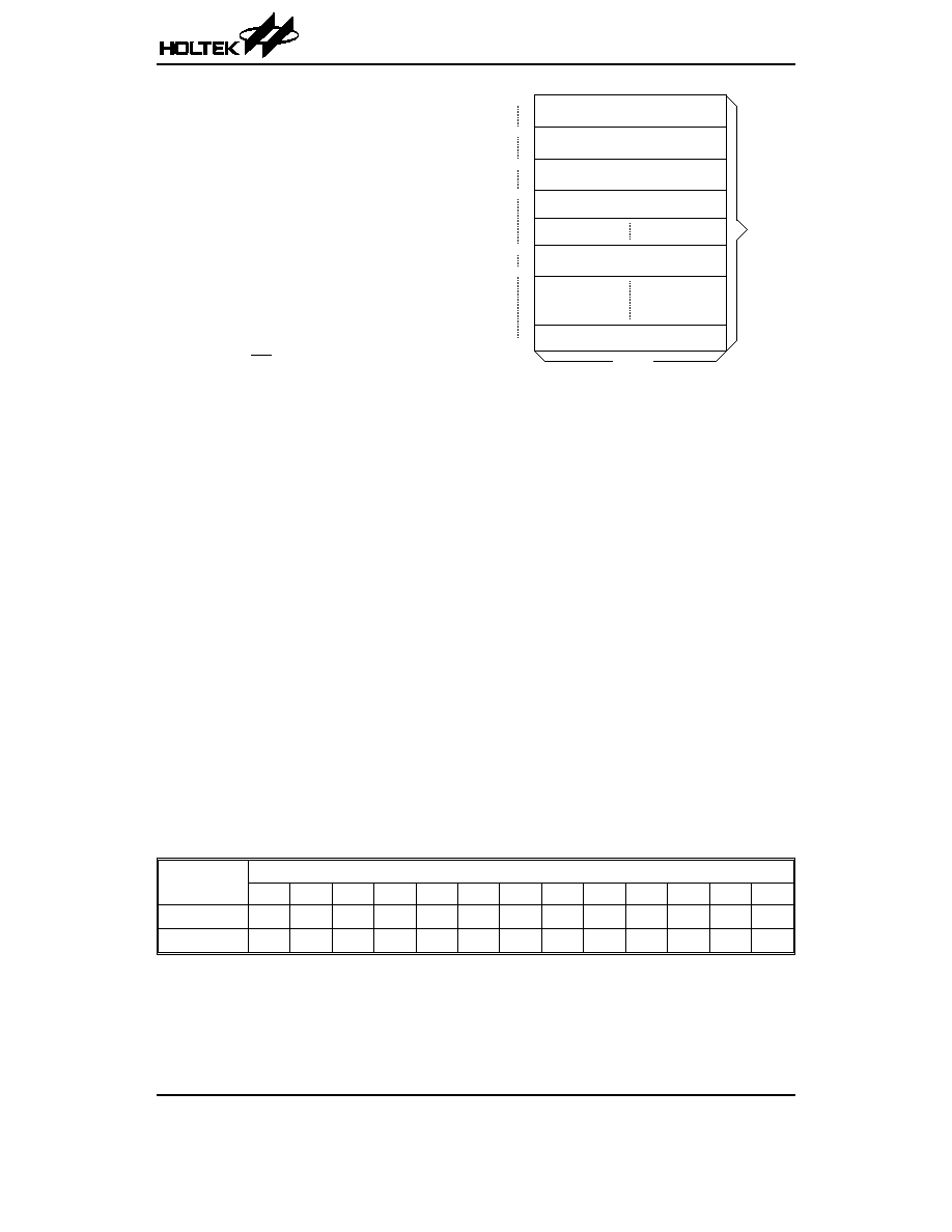
Instruction
Table Location
*12
*11
*10
*9
*8
*7
*6
*5
*4
*3
*2
*1
*0
TABRDC [m]
P12
P11
P10
P9
P8
@7
@6
@5
@4
@3
@2
@1
@0
TABRDL [m]
1
1
1
1
1
@7
@6
@5
@4
@3
@2
@1
@0
Table Location
Note: *12~*0: Table location bits
P12~P8: Current program counter bits
@7~@0: Table pointer bits
HT48R70A-1/HT48C70-1
Rev. 1.60
10
June 9, 2004
contents of the program counter are pushed onto the
stack. At the end of a subroutine or an interrupt routine,
signaled by a return instruction (RET or RETI), the pro-
gram counter is restored to its previous value from the
stack. After a chip reset, the SP will point to the top of the
stack.
If the stack is full and a non-masked interrupt takes
place, the interrupt request flag will be recorded but the
acknowledge signal will be inhibited. When the stack
pointer is decremented (by RET or RETI), the interrupt
will be serviced. This feature prevents stack overflow al-
lowing the programmer to use the structure more easily.
In a similar case, if the stack is full and a
²CALL² is sub-
sequently executed, stack overflow occurs and the first
entry will be lost (only the most recent 16 return ad-
dresses are stored).
Data Memory
- RAM
The data memory is designed with 255
´8 bits. The
data memory is divided into two functional groups: spe-
cial function registers and general purpose data mem-
ory (224
´8). Most are read/write, but some are read
only.
The special function registers include the indirect ad-
dressing registers (R0;00H, R1;02H), timer/event 0
higher order byte register (TMR0H;0CH), Timer/Event
Counter 0 lower order byte register (TMR0L; 0DH)
Timer/Event Counter 0 control register (TMR0C;0EH),
Timer/Event Counter 1 higher order byte register
(TMR1H;0FH), Timer/Event Counter 1 lower order byte
register (TMR1L;10H), Timer/Event Counter 1 control
register (TMR1C;11H), program counter lower-order
byte register (PCL;06H), memory pointer registers
(MP0;01H, MP1;03H), accumulator (ACC;05H), table
pointer (TBLP;07H), table higher-order byte register
(TBLH;08H), status register (STATUS;0AH), interrupt
control register (INTC;0BH), Watchdog Timer option
setting register (WDTS;09H), I/O registers (PA;12H,
PB;14H, PC;16H, PD;18H, PE;1AH, PF;1CH, PG;1EH)
and I/O control registers (PAC;13H, PBC;15H,
PCC;17H, PDC;19H, PEC;1BH, PFC;1DH, PGC;1FH).
The general purpose data memory, addressed from 20H
to FFH, is used for data and control information under in-
struction commands.
All of the data memory areas can handle arithmetic,
logic, increment, decrement and rotate operations di-
rectly. Except for some dedicated bits, each bit in the
data memory can be set and reset by
²SET [m].i² and
²CLR [m].i². They are also indirectly accessible through
memory pointer registers (MP0 or MP1).
Indirect Addressing Register
Location 00H and 02H are indirect addressing registers
that are not physically implemented. Any read/write op-
eration of [00H] ([02H]) will access data memory pointed
to by MP0 (MP1). Reading location 00H (02H) itself indi-
rectly will return the result 00H. Writing indirectly results
in no operation.
The memory pointer registers (MP0 and MP1) are 8-bit
registers.
Accumulator
The accumulator is closely related to ALU operations. It
is also mapped to location 05H of the data memory and
can carry out immediate data operations. The data
movement between two data memory locations must
pass through the accumulator.
G e n e r a l P u r p o s e
D A T A M E M O R Y
( 2 2 4 B y t e s )
S p e c i a l P u r p o s e
D A T A M E M O R Y
0 0 H
0 1 H
0 2 H
0 3 H
0 4 H
0 5 H
0 6 H
0 7 H
0 8 H
0 9 H
0 A H
0 B H
0 C H
0 D H
0 E H
0 F H
1 0 H
1 1 H
1 2 H
1 3 H
1 4 H
1 5 H
1 6 H
1 7 H
1 8 H
1 9 H
1 A H
1 B H
1 C H
1 D H
1 E H
1 F H
F F H
: U n u s e d
R e a d a s " 0 0 "
2 0 H
I n d i r e c t A d d r e s s i n g R e g i s t e r 0
M P 0
I n d i r e c t A d d r e s s i n g R e g i s t e r 1
M P 1
A C C
P C L
T B L P
T B L H
W D T S
S T A T U S
I N T C
T M R 0 H
T M R 0 L
T M R 0 C
T M R 1 H
T M R 1 L
T M R 1 C
P A
P A C
P B
P B C
P C
P C C
P D
P D C
P E
P E C
P F
P F C
P G
P G C
RAM Mapping
HT48R70A-1/HT48C70-1
Rev. 1.60
11
June 9, 2004
Arithmetic and Logic Unit
- ALU
This circuit performs 8-bit arithmetic and logic operations.
The ALU provides the following functions:
·
Arithmetic operations (ADD, ADC, SUB, SBC, DAA)
·
Logic operations (AND, OR, XOR, CPL)
·
Rotation (RL, RR, RLC, RRC)
·
Increment and Decrement (INC, DEC)
·
Branch decision (SZ, SNZ, SIZ, SDZ ....)
The ALU not only saves the results of a data operation but
also changes the status register.
Status Register
- STATUS
This 8-bit register (0AH) contains the zero flag (Z), carry
flag (C), auxiliary carry flag (AC), overflow flag (OV),
power down flag (PDF), and watchdog time-out flag
(TO). It also records the status information and controls
the operation sequence.
With the exception of the TO and PDF flags, bits in
the status register can be altered by instructions like
most other registers. Any data written into the status
register will not change the TO or PDF flag. In addi-
tion operations related to the status register may give
different results from those intended. The TO flag
can be affected only by system power-up, a WDT
time-out or executing the
²CLR WDT² or ²HALT² in-
struction. The PDF flag can be affected only by exe-
cuting the
²HALT² or ²CLR WDT² instruction or
during a system power-up.
The Z, OV, AC and C flags generally reflect the status of
the latest operations.
In addition, on entering the interrupt sequence or exe-
cuting the subroutine call, the status register will not be
pushed onto the stack automatically. If the contents of
the status are important and if the subroutine can cor-
rupt the status register, precautions must be taken to
save it properly.
Interrupt
The device provides an external interrupt and internal
timer/event counter interrupts. The Interrupt Control
Register (INTC;0BH) contains the interrupt control bits
to set the enable or disable and the interrupt request
flags.
Once an interrupt subroutine is serviced, all the other in-
terrupts will be blocked (by clearing the EMI bit). This
scheme may prevent any further interrupt nesting. Other
interrupt requests may occur during this interval but only
the interrupt request flag is recorded. If a certain inter-
rupt requires servicing within the service routine, the
EMI bit and the corresponding bit of the INTC may be set
to allow interrupt nesting. If the stack is full, the interrupt
request will not be acknowledged, even if the related in-
terrupt is enabled, until the SP is decremented. If immedi-
ate service is desired, the stack must be prevented from
becoming full.
All these kinds of interrupts have a wake-up capability.
As an interrupt is serviced, a control transfer occurs by
pushing the program counter onto the stack, followed by
a branch to a subroutine at specified location in the pro-
gram memory. Only the program counter is pushed onto
the stack. If the contents of the register or status register
(STATUS) are altered by the interrupt service program
which corrupts the desired control sequence, the con-
tents should be saved in advance.
External interrupts are triggered by a high to low transi-
tion of the INT and the related interrupt request flag (EIF;
bit 4 of INTC) will be set. When the interrupt is enabled,
the stack is not full and the external interrupt is active, a
subroutine call to location 04H will occur. The interrupt
request flag (EIF) and EMI bits will be cleared to disable
other interrupts.
The internal Timer/Event Counter 0 interrupt is initial-
ized by setting the Timer/Event Counter 0 interrupt re-
quest flag (T0F; bit 5 of INTC), caused by a timer 0
overflow. When the interrupt is enabled, the stack is not
full and the T0F bit is set, a subroutine call to location
Labels
Bits
Function
C
0
C is set if the operation results in a carry during an addition operation or if a borrow does not take
place during a subtraction operation; otherwise C is cleared. C is also affected by a rotate
through carry instruction.
AC
1
AC is set if the operation results in a carry out of the low nibbles in addition or no borrow from the
high nibble into the low nibble in subtraction; otherwise AC is cleared.
Z
2
Z is set if the result of an arithmetic or logic operation is zero; otherwise Z is cleared.
OV
3
OV is set if the operation results in a carry into the highest-order bit but not a carry out of the
highest-order bit, or vice versa; otherwise OV is cleared.
PDF
4
PDF is cleared by system power-up or executing the
²CLR WDT² instruction. PDF is set by exe-
cuting the
²HALT² instruction.
TO
5
TO is cleared by system power-up or executing the
²CLR WDT² or HALT instruction. TO is set
by a WDT time-out.
¾
6, 7
Unused bit, read as
²0²
Status Register
HT48R70A-1/HT48C70-1
Rev. 1.60
12
June 9, 2004
08H will occur. The related interrupt request flag (T0F)
will be reset and the EMI bit cleared to disable further in-
terrupts.
The internal timer/even counter 1 interrupt is initialized
by setting the Timer/Event Counter 1 interrupt request
flag (T1F;bit 6 of INTC), caused by a timer 1 overflow.
When the interrupt is enabled, the stack is not full and
the T1F is set, a subroutine call to location 0CH will oc-
cur. The related interrupt request flag (T1F) will be reset
and the EMI bit cleared to disable further interrupts.
During the execution of an interrupt subroutine, other in-
terrupt acknowledge signals are held until the
²RETI² in-
struction is executed or the EMI bit and the related
interrupt control bit are set to 1 (if the stack is not full). To
return from the interrupt subroutine,
²RET² or ²RETI²
may be invoked. RETI will set the EMI bit to enable an in-
terrupt service, but RET will not.
Interrupts, occurring in the interval between the rising
edges of two consecutive T2 pulses, will be serviced on
the latter of the two T2 pulses, if the corresponding inter-
rupts are enabled. In the case of simultaneous requests
the following table shows the priority that is applied.
These can be masked by resetting the EMI bit.
No.
Interrupt Source
Priority Vector
a
External Interrupt
1
04H
b
Timer/Event Counter 0 Overflow
2
08H
c
Timer/Event Counter 1 Overflow
3
0CH
The Timer/Event Counter 0/1 interrupt request flag
(T0F/T1F), external interrupt request flag (EIF), enable
Timer/Event Counter 0/1 interrupt bit (ET0I/ET1I), en-
able external interrupt bit (EEI) and enable master inter-
rupt bit (EMI) constitute an interrupt control register
(INTC) which is located at 0BH in the data memory. EMI,
EEI, ET0I and ET1I are used to control the enabling or
disabling of interrupts. These bits prevent the requested
interrupt from being serviced. Once the interrupt request
flags (T0F, T1F, EIF) are set, they will remain in the INTC
register until the interrupts are serviced or cleared by a
software instruction.
It is recommended that a program does not use the
²CALL subroutine² within the interrupt subroutine. In-
terrupts often occur in an unpredictable manner or
need to be serviced immediately in some applications.
If only one stack is left and enabling the interrupt is not
well controlled, the original control sequence will be dam-
aged once the
²CALL² operates in the interrupt subrou-
tine.
Oscillator Configuration
There are 3 oscillator circuits in the microcontroller.
All of them are designed for system clocks, namely the
external RC oscillator, the external Crystal oscillator and
the internal RC oscillator, which are determined by op-
tions. No matter what oscillator type is selected, the sig-
nal provides the system clock. The HALT mode stops
the system oscillator and ignores an external signal to
conserve power.
If an RC oscillator is used, an external resistor between
OSC1 and VDD is required and the resistance must
range from 24k
W to 1MW. The system clock, divided by
4, is available on OSC2, which can be used to synchro-
nize external logic. The RC oscillator provides the most
cost effective solution. However, the frequency of oscil-
lation may vary with VDD, temperatures and the chip it-
self due to process variations. It is, therefore, not
suitable for timing sensitive operations where an accu-
rate oscillator frequency is desired.
If the Crystal oscillator is used, a crystal across OSC1
and OSC2 is needed to provide the feedback and phase
shift required for the oscillator. No other external compo-
nents are required. In stead of a crystal, a resonator can
also be connected between OSC1 and OSC2 to get a
Register
Bit No.
Label
Function
INTC
(0BH)
0
EMI
Controls the master (global) interrupt (1= enabled; 0= disabled)
1
EEI
Controls the external interrupt (1= enabled; 0= disabled)
2
ET0I
Controls the Timer/Event Counter 0 interrupt (1= enabled; 0= disabled)
3
ET1I
Controls the Timer/Event Counter 1 interrupt (1= enabled; 0= disabled)
4
EIF
External interrupt request flag (1= active; 0= inactive)
5
T0F
Internal Timer/Event Counter 0 request flag (1= active; 0= inactive)
6
T1F
Internal Timer/Event Counter 1 request flag (1= active; 0= inactive)
7
¾
Unused bit, read as
²0²
INTC Register
C r y s t a l O s c i l l a t o r
( I n c l u d e 3 2 7 6 8 H z )
R C O s c i l l a t o r
O S C 1
O S C 2
N M O S O p e n D r a i n
O S C 2
f
S Y S
/ 4
4 7 0 p F
V
D D
O S C 1
System Oscillator

HT48R70A-1/HT48C70-1
Rev. 1.60
13
June 9, 2004
frequency reference, but two external capacitors in
OSC1 and OSC2 are required. If the internal RC oscilla-
tor is used, the OSC1 and OSC2 can be selected as
32768Hz crystal oscillator (RTC OSC). Also, the fre-
quencies of the internal RC oscillator can be 3.2MHz,
1.6MHz, 800kHz and 400kHz (depends on the options).
The WDT oscillator is a free running on-chip RC oscilla-
tor, and no external components are required. Even if
the system enters the power down mode, the system
clock is stopped, but the WDT oscillator still works within
a period of approximately 65
ms@5V. The WDT oscillator
can be disabled by options to conserve power.
Watchdog Timer
- WDT
The WDT clock source is implemented by a dedicated
RC oscillator (WDT oscillator), RTC clock or instruction
clock (system clock divided by 4), determines the op-
tions. This timer is designed to prevent a software mal-
function or sequence from jumping to an unknown
location with unpredictable results. The Watchdog
Timer can be disabled by options. If the Watchdog Timer
is disabled, all the executions related to the WDT result
in no operation. The RTC clock is enabled only in the in-
ternal RC+RTC mode.
Once the internal WDT oscillator (RC oscillator with a
period of 65
ms@5V normally) is selected, it is first di-
vided by 256 (8-stage) to get the nominal time-out pe-
riod of 17ms@5V. This time-out period may vary with
temperatures, VDD and process variations. By invoking
the WDT prescaler, longer time-out periods can be real-
ized. Writing data to WS2, WS1, WS0 (bit 2,1,0 of the
WDTS) can give different time-out periods. If WS2,
WS1, and WS0 are all equal to 1, the division ratio is up
to 1:128, and the maximum time-out period is 2.1s@5V
seconds. If the WDT oscillator is disabled, the WDT
clock may still come from the instruction clock and oper-
ates in the same manner except that in the HALT state
the WDT may stop counting and lose its protecting pur-
pose. In this situation the logic can only be restarted by
external logic. The high nibble and bit 3 of the WDTS are
reserved for users defined flags, which can be used to
indicate some specified status.
If the device operates in a noisy environment, using the
on-chip RC oscillator (WDT OSC) or 32kHz crystal oscil-
lator (RTC OSC) is strongly recommended, since the
HALT will stop the system clock.
WS2
WS1
WS0
Division Ratio
0
0
0
1:1
0
0
1
1:2
0
1
0
1:4
0
1
1
1:8
1
0
0
1:16
1
0
1
1:32
1
1
0
1:64
1
1
1
1:128
WDTS Register
The WDT overflow under normal operation will initialize
²chip reset² and set the status bit ²TO². But in the HALT
mode, the overflow will initialize a
²warm reset² and only
the PC and SP are reset to zero. To clear the contents of
WDT (including the WDT prescaler), three methods are
adopted; external reset (a low level to RES), software in-
struction and a
²HALT² instruction. The software instruc-
tion include
²CLR WDT² and the other set - ²CLR
WDT1
² and ²CLR WDT2². Of these two types of instruc-
tion, only one can be active depending on the option
-
²CLR WDT times selection option². If the ²CLR WDT² is
selected (i.e. CLRWDT times equal one), any execution
of the
²CLR WDT² instruction will clear the WDT. In the
case that
²CLR WDT1² and ²CLR WDT2² are chosen
(i.e. CLRWDT times equal two), these two instructions
must be executed to clear the WDT; otherwise, the WDT
may reset the chip as a result of time-out.
Power Down Operation
- HALT
The HALT mode is initialized by the
²HALT² instruction
and results in the following...
·
The system oscillator will be turned off but the WDT
oscillator remains running (if the WDT oscillator is se-
lected).
·
The contents of the on chip RAM and registers remain
unchanged.
·
WDT and WDT prescaler will be cleared and re-
counted again (if the WDT clock is from the WDT os-
cillator).
·
All of the I/O ports maintain their original status.
·
The PDF flag is set and the TO flag is cleared.
The system can leave the HALT mode by means of an
external reset, an interrupt, an external falling edge sig-
nal on port A or a WDT overflow. An external reset
S y s t e m C l o c k / 4
8 - b i t C o u n t e r
W D T P r e s c a l e r
7 - b i t C o u n t e r
8 - t o - 1 M U X
W D T T i m e - o u t
W S 0 ~ W S 2
O p t i o n
S e l e c t
W D T
O S C
R T C O S C
Watchdog Timer
HT48R70A-1/HT48C70-1
Rev. 1.60
14
June 9, 2004
causes a device initialization and the WDT overflow per-
forms a
²warm reset². After the TO and PDF flags are
examined, the reason for chip reset can be determined.
The PDF flag is cleared by system power-up or execut-
ing the
²CLR WDT² instruction and is set when execut-
ing the
²HALT² instruction. The TO flag is set if the WDT
time-out occurs, and causes a wake-up that only resets
the PC and SP; the others remain in their original status.
The port A wake-up and interrupt methods can be con-
sidered as a continuation of normal execution. Each bit
in port A can be independently selected to wake-up the
device by options. Awakening from an I/O port stimulus,
the program will resume execution of the next instruc-
tion. If it awakens from an interrupt, two sequence may
occur. If the related interrupt is disabled or the interrupt
is enabled but the stack is full, the program will resume
execution at the next instruction. If the interrupt is en-
abled and the stack is not full, the regular interrupt re-
sponse takes place. If an interrupt request flag is set to
²1² before entering the HALT mode, the wake-up func-
tion of the related interrupt will be disabled. Once a
wake-up event occurs, it takes 1024 t
SYS
(system clock
period) to resume normal operation. In other words, a
dummy period will be inserted after a wake-up. If the
wake-up results from an interrupt acknowledge signal,
the actual interrupt subroutine execution will be delayed
by one or more cycles. If the wake-up results in the next
instruction execution, this will be executed immediately
after the dummy period is finished.
To minimize power consumption, all the I/O pins should
be carefully managed before entering the HALT status.
The RTC oscillator still runs in the HALT mode (if the
RTC oscillator is enabled).
Reset
There are three ways in which a reset can occur:
·
RES reset during normal operation
·
RES reset during HALT
·
WDT time-out reset during normal operation
The WDT time-out during HALT is different from other
chip reset conditions, since it can perform a
²warm re -
set
² that resets only the PC and SP, leaving the other cir-
cuits in their original state. Some registers remain un-
changed during other reset conditions. Most registers
are reset to the
²initial condition² when the reset condi-
tions are met. By examining the PDF and TO flags, the
program can distinguish between different
²chip resets².
TO PDF
RESET Conditions
0
0
RES reset during power-up
u
u
RES reset during normal operation
0
1
RES wake-up HALT
1
u
WDT time-out during normal operation
1
1
WDT wake-up HALT
Note:
²u² stands for ²unchanged²
To guarantee that the system oscillator is started and
stabilized, the SST (System Start-up Timer) provides an
extra-delay of 1024 system clock pulses when the sys-
tem reset (power-up, WDT time-out or RES reset) or the
system awakes from the HALT state.
When a system reset occurs, the SST delay is added
during the reset period. Any wake-up from HALT will en-
able the SST delay.
An extra option load time delay is added during system
reset (power-up, WDT time-out at normal mode or RES
reset).
The functional unit chip reset status are shown below.
PC
000H
Interrupt
Disable
Prescaler
Clear
WDT
Clear. After master reset,
WDT begins counting
Timer/Event Counter
Off
Input/Output Ports
Input mode
SP
Points to the top of the stack
R E S
V
D D
1 0 0 k W
1 0 k W
0 . 1 m F *
0 . 0 1 m F *
Reset Circuit
Note:
²*² Make the length of the wiring, which is con-
nected to the RES pin as short as possible, to
avoid noise interference.
W a r m R e s e t
W D T
H A L T
C o l d
R e s e t
R E S
S y s t e m R e s e t
S S T
1 0 - b i t R i p p l e
C o u n t e r
O S C 1
Reset Configuration
t
S S T
R E S
V D D
S S T T i m e - o u t
C h i p R e s e t
Reset Timing Chart
HT48R70A-1/HT48C70-1
Rev. 1.60
15
June 9, 2004
The states of the registers is summarized in the table.
Register
Reset
(Power On)
WDT Time-out
(Normal Operation)
RES Reset
(Normal Operation)
RES Reset
(HALT)
WDT Time-out
(HALT)*
TMR0H
xxxx xxxx
xxxx xxxx
xxxx xxxx
xxxx xxxx
uuuu uuuu
TMR0L
xxxx xxxx
xxxx xxxx
xxxx xxxx
xxxx xxxx
uuuu uuuu
TMR0C
00-0 1---
00-0 1---
00-0 1---
00-0 1---
uu-u u---
TMR1H
xxxx xxxx
xxxx xxxx
xxxx xxxx
xxxx xxxx
uuuu uuuu
TMR1L
xxxx xxxx
xxxx xxxx
xxxx xxxx
xxxx xxxx
uuuu uuuu
TMR1C
00-0 1---
00-0 1---
00-0 1---
00-0 1---
uu-u u---
Program
Counter
000H
000H
000H
000H
000H
MP0
xxxx xxxx
uuuu uuuu
uuuu uuuu
uuuu uuuu
uuuu uuuu
MP1
xxxx xxxx
uuuu uuuu
uuuu uuuu
uuuu uuuu
uuuu uuuu
ACC
xxxx xxxx
uuuu uuuu
uuuu uuuu
uuuu uuuu
uuuu uuuu
TBLP
xxxx xxxx
uuuu uuuu
uuuu uuuu
uuuu uuuu
uuuu uuuu
TBLH
xxxx xxxx
uuuu uuuu
uuuu uuuu
uuuu uuuu
uuuu uuuu
STATUS
--00 xxxx
--1u uuuu
--uu uuuu
--01 uuuu
--11 uuuu
INTC
-000 0000
-000 0000
-000 0000
-000 0000
-uuu uuuu
WDTS
0000 0111
0000 0111
0000 0111
0000 0111
uuuu uuuu
PA
1111 1111
1111 1111
1111 1111
1111 1111
uuuu uuuu
PAC
1111 1111
1111 1111
1111 1111
1111 1111
uuuu uuuu
PB
1111 1111
1111 1111
1111 1111
1111 1111
uuuu uuuu
PBC
1111 1111
1111 1111
1111 1111
1111 1111
uuuu uuuu
PC
1111 1111
1111 1111
1111 1111
1111 1111
uuuu uuuu
PCC
1111 1111
1111 1111
1111 1111
1111 1111
uuuu uuuu
PD
1111 1111
1111 1111
1111 1111
1111 1111
uuuu uuuu
PDC
1111 1111
1111 1111
1111 1111
1111 1111
uuuu uuuu
PE
1111 1111
1111 1111
1111 1111
1111 1111
uuuu uuuu
PEC
1111 1111
1111 1111
1111 1111
1111 1111
uuuu uuuu
PF
1111 1111
1111 1111
1111 1111
1111 1111
uuuu uuuu
PFC
1111 1111
1111 1111
1111 1111
1111 1111
uuuu uuuu
PG
1111 1111
1111 1111
1111 1111
1111 1111
uuuu uuuu
PGC
1111 1111
1111 1111
1111 1111
1111 1111
uuuu uuuu
Note:
²*² stands for ²warm reset²
²u² stands for ²unchanged²
²x² stands for ²unknown²

HT48R70A-1/HT48C70-1
Rev. 1.60
16
June 9, 2004
Timer/Event Counter
Two timer/event counters (TMR0, TMR1) are imple-
mented in the microcontroller. The Timer/Event Counter
0 contains an 16-bit programmable count-up counter
and the clock may come from an external source or from
the system clock divided by 4 or RTC.
The Timer/Event Counter 1 contains an 16-bit program-
mable count-up counter and the clock may come from
an external source or from the system clock divided by 4
or RTC.
Using the internal clock sources, there are 2 reference
time-bases for Timer/Event Counter 0. The internal
clock source can be selected as coming from f
TID
(can
always be optioned) or f
RTC
(enabled only system oscil-
lator in the Int. RC+RTC mode) by options.
Using the internal clock sources, there are 2 reference
time-bases for Timer/Event Counter 1. The internal
clock source can be selected as coming from f
SYS
/4
(can always be optioned) or f
RTC
(enable only the sys-
tem oscillator in the Int. RC+RTC mode) by options.
Using external clock input allows the user to count exter-
nal events, measure time internals or pulse widths, or
generate an accurate time base. While using the inter-
nal clock allows the user to generate an accurate time
base.
There are 3 registers related to the Timer/Event Counter
0;TMR0H ([0CH]), TMR0L ([0DH]), TMR0C ([0EH]). Writ-
ing TMR0L will only put the written data to an internal
lower-order byte buffer (8 bits) and writing TMR0H will
transfer the specified data and the contents of the
lower-order byte buffer to TMR0H and TMR0L preload
registers, respectively. The Timer/Event Counter 1 preload
register is changed by each writing TMR0H operations.
Reading TMR0H will latch the contents of TMR0H and
TMR0L counters to the destination and the lower-order
byte buffer, respectively. Reading the TMR0L will read the
contents of the lower-order byte buffer. The TMR0C is the
Timer/Event Counter 1 control register, which defines the
operating mode, counting enable or disable and active
edge.
There are 3 registers related to Timer/Event Counter 1;
TMR1H (0FH), TMR1L (10H), TMR1C (11H). Writing
TMR1L will only put the written data to an internal
lower-order byte buffer (8 bits) and writing TMR1H will
transfer the specified data and the contents of the
lower-order byte buffer to TMR1H and TMR1L preload
registers, respectively. The Timer/Event Counter 1
preload register is changed by each writing TMR1H op-
erations. Reading TMR1H will latch the contents of
TMR1H and TMR1L counters to the destination and the
Label (TMR0C)
Bits
Function
¾
0~2
Unused bit, read as
²0²
T0E
3
To define the TMR0 active edge of Timer/Event Counter 0
(0=active on low to high; 1=active on high to low)
T0ON
4
To enable or disable timer 0 counting
(0=disabled; 1=enabled)
¾
5
Unused bit, read as
²0²
T0M0
T0M1
6
7
To define the operating mode
01=Event count mode (external clock)
10=Timer mode (internal clock)
11=Pulse width measurement mode
00=Unused
TMR0C Register
Label (TMR1C)
Bits
Function
¾
0~2
Unused bit, read as
²0²
T1E
3
To define the TMR1 active edge of Timer/Event Counter 1
(0=active on low to high; 1=active on high to low)
T1ON
4
To enable or disable timer 1 counting
(0=disabled; 1=enabled)
¾
5
Unused bit, read as
²0²
T1M0
T1M1
6
7
To define the operating mode
01=Event count mode (external clock)
10=Timer mode (internal clock)
11=Pulse width measurement mode
00=Unused
TMR1C Register
HT48R70A-1/HT48C70-1
Rev. 1.60
17
June 9, 2004
lower-order byte buffer, respectively. Reading the
TMR1L will read the contents of the lower-order byte
buffer. The TMR1C is the Timer/Event Counter 1 control
register, which defines the operating mode, counting
enable or disable and active edge.
The T0M0, T0M1 (TMR0C), T1M0, T1M1 (TMR1C) bits
define the operating mode. The event count mode is
used to count external events, which means the clock
source comes from an external (TMR0/TMR1) pin. The
timer mode functions as a normal timer with the clock
source coming from the instruction clock or RTC clock
(Timer0/Timer1). The pulse width measurement mode
can be used to count the high or low level duration of the
external signal (TMR0/TMR1). The counting is based on
the instruction clock or RTC clock (Timer0/Timer1).
In the event count or timer mode, once the Timer/Event
Counter 0/1 starts counting, it will count from the current
contents in the Timer/Event Counter 0/1 to FFFFH.
Once overflow occurs, the counter is reloaded from the
Timer/Event Counter 0/1 preload register and generates
the interrupt request flag (T0F/T1F; bit 5/6 of INTC) at
the same time.
In the pulse width measurement mode with the
T0ON/T1ON and T0E/T1E bits equal to one, once the
TMR0/TMR1 has received a transient from low to high
(or high to low if the T0E/T1E bits is
²0²) it will start
counting until the TMR0/TMR1 returns to the original
level and resets the T0ON/T1ON. The measured result
will remain in the Timer/Event Counter 0/1 even if the
activated transient occurs again. In other words, only
one cycle measurement can be done. Until setting the
T0ON/T1ON, the cycle measurement will function again
as long as it receives further transient pulse. Note that,
in this operating mode, the Timer/Event Counter 0/1
starts counting not according to the logic level but ac-
cording to the transient edges. In the case of counter
overflows, the counter 0/1 is reloaded from the
Timer/Event Counter 0/1 preload register and issues the
interrupt request just like the other two modes. To en-
able the counting operation, the timer ON bit (T0ON: bit
4 of TMR0C; T1ON: bit 4 of TMR1C) should be set to 1.
In the pulse width measurement mode, the T0ON/T1ON
will be cleared automatically after the measurement cy-
cle is completed. But in the other two modes the
T0ON/T1ON can only be reset by instructions. The
overflow of the Timer/Event Counter 0/1 is one of the
wake-up sources. No matter what the operation mode
is, writing a 0 to ET0I/ET1I can disable the correspond-
ing interrupt services.
In the case of Timer/Event Counter 0/1 OFF condition,
writing data to the Timer/Event Counter 0/1 preload
register will also reload that data to the Timer/Event
Counter 0/1. But if the Timer/Event Counter 0/1 is turned
on, data written to it will only be kept in the Timer/Event
Counter 0/1 preload register. The Timer/Event Counter
0/1 will still operate until overflow occurs (a Timer/Event
Counter 0/1 reloading will occur at the same time). When
the Timer/Event Counter 0/1 (reading TMR0/TMR1) is
read, the clock will be blocked to avoid errors. As clock
blocking may results in a counting error, this must be
taken into consideration by the programmer.
T 1 M 1
T 1 M 0
T M R 1
T 1 E
T 1 M 1
T 1 M 0
T 1 O N
P u l s e W i d t h
M e a s u r e m e n t
M o d e C o n t r o l
1 6 B i t s
T i m e r / E v e n t C o u n t e r
P r e l o a d R e g i s t e r
D a t a B u s
R e l o a d
O v e r f l o w
t o I n t e r r u p t
f
S Y S / 4
M
U
X
f
R T C
O p t i o n
1 6 B i t s
T i m e r / E v e n t C o u n t e r
( T M R 1 H / T M R 1 L )
L o w B y t e
B u f f e r
Timer/Event Counter 1
T 0 M 1
T 0 M 0
T M R 0
T 0 E
T 0 M 1
T 0 M 0
T 0 O N
P u l s e W i d t h
M e a s u r e m e n t
M o d e C o n t r o l
1 6 B i t s
T i m e r / E v e n t C o u n t e r
P r e l o a d R e g i s t e r
D a t a B u s
R e l o a d
O v e r f l o w
t o I n t e r r u p t
f
S Y S / 4
M
U
X
f
R T C
O p t i o n
1 6 B i t s
T i m e r / E v e n t C o u n t e r
( T M R 0 H / T M R 0 L )
L o w B y t e
B u f f e r
Timer/Event Counter 0
HT48R70A-1/HT48C70-1
Rev. 1.60
18
June 9, 2004
Input/Output Ports
There are 56 bidirectional input/output lines in the
microcontroller, labeled from PA to PG, which are
mapped to the data memory of [12H], [14H], [16H],
[18H], [1AH], [1CH] and [1EH] respectively. All of these
I/O ports can be used for input and output operations.
For input operation, these ports are non-latching, that is,
the inputs must be ready at the T2 rising edge of
instruction
²MOV A,[m]² (m=12H, 14H, 16H, 18H, 1AH,
1CH or 1EH). For output operation, all the data is
latched and remains unchanged until the output latch is
rewritten.
Each I/O line has its own control register (PAC, PBC,
PCC, PDC, PEC, PFC, PGC) to control the input/output
configuration. With this control register, CMOS output or
Schmitt trigger input with or without pull-high resistor
structures can be reconfigured dynamically (i.e.
on-the-fly) under software control. To function as an in-
put, the corresponding latch of the control register must
write
²1². The input source also depends on the control
register. If the control register bit is
²1², the input will
read the pad state. If the control register bit is
²0², the
contents of the latches will move to the internal bus. The
latter is possible in the
²read-modify-write² instruction.
For output function, CMOS is the only configuration.
These control registers are mapped to locations 13H,
15H, 17H, 19H, 1BH, 1DH and 1FH.
After a chip reset, these input/output lines remain at high
levels or floating state (depending on the pull-high op-
tions). Each bit of these input/output latches can be set
or cleared by
²SET [m].i² and ²CLR [m].i² (m=12H, 14H,
16H, 18H, 1AH, 1CH or 1EH) instructions.
Some instructions first input data and then follow the
output operations. For example,
²SET [m].i², ²CLR
[m].i
², ²CPL [m]², ²CPLA [m]² read the entire port states
into the CPU, execute the defined operations
(bit-operation), and then write the results back to the
latches or the accumulator.
Each line of port A has the capability of waking-up the
device.
There is a pull-high option available for all I/O lines (port
option). Once the pull-high option of an I/O line is se-
lected, the I/O line have pull-high resistor. Otherwise,
the pull-high resistor is absent. It should be noted that a
non-pull-high I/O line operating in input mode will cause
a floating state.
V
D D
P A 0 ~ P A 7
P B 0 ~ P B 7
P C 0 ~ P C 7
P D 0 ~ P D 7
P E 0 ~ P E 7
P F 0 ~ P F 7
P G 0 ~ P G 7
M
U
X
O P 0 ~ O P 7
S y s t e m W a k e - u p
( P A o n l y )
R e a d D a t a R e g i s t e r
D
Q
C K
S
D
Q
C K
S
C o n t r o l B i t
P U
D a t a B u s
W r i t e C o n t r o l R e g i s t e r
C h i p R e s e t
R e a d C o n t r o l R e g i s t e r
W r i t e D a t a R e g i s t e r
D a t a B i t
Q
Q
Input/Output Ports
HT48R70A-1/HT48C70-1
Rev. 1.60
19
June 9, 2004
Low Voltage Reset
- LVR
The microcontroller provides low voltage reset circuit in
order to monitor the supply voltage of the device. If the
supply voltage of the device is within the range
0.9V~V
LVR
, such as changing a battery, the LVR will au-
tomatically reset the device internally.
The LVR includes the following specifications:
·
The low voltage (0.9V~V
LVR
) has to remain in their
original state to exceed 1ms. If the low voltage state
does not exceed 1ms, the LVR will ignore it and do not
perform a reset function.
·
The LVR uses the
²OR² function with the external
RES signal to perform chip reset.
The relationship between V
DD
and V
LVR
is shown below.
Note:
V
OPR
is the voltage range for proper chip opera-
tion at 4MHz system clock.
5 . 5 V
3 . 0 V
2 . 2 V
0 . 9 V
V
D D
V
O P R
V
L V R
5 . 5 V
V
D D
5 . 5 V
V
L V R
0 . 9 V
0 V
R e s e t S i g n a l
R e s e t
* 1
* 2
N o r m a l O p e r a t i o n
R e s e t
L V R D e t e c t V o l t a g e
Low Voltage Reset
Note:
*1: To make sure that the system oscillator has stabilized, the SST provides an extra delay of
1024 system clock pulses before entering the normal operation.
*2: Since low voltage has to be maintained in its original state and exceed 1ms, therefore 1ms
delay enters the reset mode.
Options
The following table shows all kinds of options in the microcontroller. All of the options must be defined to ensure proper
system functioning.
No.
Options
1
WDT clock source: WDT oscillator or f
SYS
/4 or RTC oscillator or disable
2
CLRWDT instructions: 1 or 2 instructions
3
Timer/Event Counter 0 clock sources: f
SYS
/4 or RTCOSC
4
Timer/Event Counter 1 clock sources: f
SYS
/4 or RTCOSC
5
PA bit wake-up enable or disable
6
PA CMOS or Schmitt input
7
PA, PB, PC, PD, PE, PF, PG pull-high enable or disable (By port)
8
System oscillator
Ext. RC, Ext. crystal, Int. RC+RTC
9
Int. RC frequency selection 3.2MHz, 1.6MHz, 800kHz or 400kHz
10
LVR enable or disable
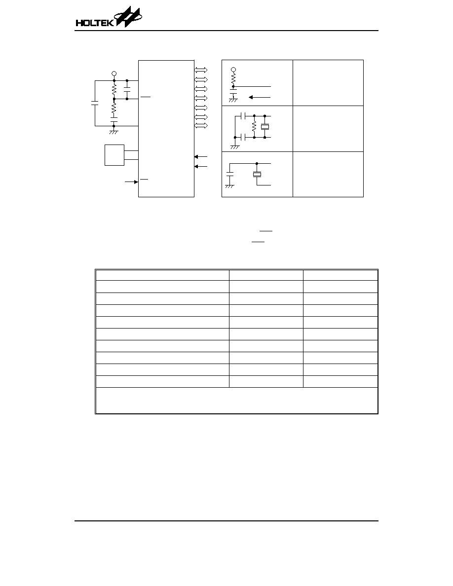
Application Circuits
Note:
The resistance and capacitance for reset circuit should be designed to ensure that the VDD is stable and re-
mains in a valid range of the operating voltage before bringing RES to high.
²*² Make the length of the wiring, which is connected to the RES pin as short as possible, to avoid noise
interference.
The following table shows the C1, C2 and R1 value according different crystal values. (For reference only)
Crystal or Resonator
C1, C2
R1
4MHz Crystal
0pF
10k
W
4MHz Resonator
10pF
12k
W
3.58MHz Crystal
0pF
10k
W
3.58MHz Resonator
25pF
10k
W
2MHz Crystal & Resonator
25pF
10k
W
1MHz Crystal
35pF
27k
W
480kHz Resonator
300pF
9.1k
W
455kHz Resonator
300pF
10k
W
429kHz Resonator
300pF
10k
W
The function of the resistor R1 is to ensure that the oscillator will switch off should low voltage condi-
tions occur. Such a low voltage, as mentioned here, is one which is less than the lowest value of the
MCU operating voltage. Note however that if the LVR is enabled then R1 can be removed.
HT48R70A-1/HT48C70-1
Rev. 1.60
20
June 9, 2004
O S C 1
O S C 2
C r y s t a l S y s t e m O s c i l l a t o r
F o r t h e v a l u e s ,
s e e t a b l e b e l o w
R C S y s t e m O s c i l l a t o r
2 4 k W < R
O S C
< 1 M W
R 1
C 1
C 2
V
D D
R
O S C
O S C 1
O S C 2
4 7 0 p F
N M O S o p e n d r a i n
O S C 1
O S C 2
O S C
C i r c u i t
R E S
0 . 1 m F *
1 0 0 k W
V D D
V S S
0 . 1 m F
V
D D
0 . 0 1 m F *
1 0 k W
O S C C i r c u i t
I n t e r n a l R C O s c i l l a t o r
w i t h R T C
H T 4 8 R 7 0 A - 1 / H T 4 8 C 7 0 - 1
P A 0 ~ P A 7
P B 0 ~ P B 7
P C 0 ~ P C 7
P D 0 ~ P D 7
T M R 0
T M R 1
P E 0 ~ P E 7
P F 0 ~ P F 7
P G 0 ~ P G 7
I N T
O S C 1
O S C 2
3 2 7 6 8 H z
1 0 p F
S e e R i g h t S i d e
Instruction Set Summary
Mnemonic
Description
Instruction
Cycle
Flag
Affected
Arithmetic
ADD A,[m]
ADDM A,[m]
ADD A,x
ADC A,[m]
ADCM A,[m]
SUB A,x
SUB A,[m]
SUBM A,[m]
SBC A,[m]
SBCM A,[m]
DAA [m]
Add data memory to ACC
Add ACC to data memory
Add immediate data to ACC
Add data memory to ACC with carry
Add ACC to data memory with carry
Subtract immediate data from ACC
Subtract data memory from ACC
Subtract data memory from ACC with result in data memory
Subtract data memory from ACC with carry
Subtract data memory from ACC with carry and result in data memory
Decimal adjust ACC for addition with result in data memory
1
1
(1)
1
1
1
(1)
1
1
1
(1)
1
1
(1)
1
(1)
Z,C,AC,OV
Z,C,AC,OV
Z,C,AC,OV
Z,C,AC,OV
Z,C,AC,OV
Z,C,AC,OV
Z,C,AC,OV
Z,C,AC,OV
Z,C,AC,OV
Z,C,AC,OV
C
Logic Operation
AND A,[m]
OR A,[m]
XOR A,[m]
ANDM A,[m]
ORM A,[m]
XORM A,[m]
AND A,x
OR A,x
XOR A,x
CPL [m]
CPLA [m]
AND data memory to ACC
OR data memory to ACC
Exclusive-OR data memory to ACC
AND ACC to data memory
OR ACC to data memory
Exclusive-OR ACC to data memory
AND immediate data to ACC
OR immediate data to ACC
Exclusive-OR immediate data to ACC
Complement data memory
Complement data memory with result in ACC
1
1
1
1
(1)
1
(1)
1
(1)
1
1
1
1
(1)
1
Z
Z
Z
Z
Z
Z
Z
Z
Z
Z
Z
Increment & Decrement
INCA [m]
INC [m]
DECA [m]
DEC [m]
Increment data memory with result in ACC
Increment data memory
Decrement data memory with result in ACC
Decrement data memory
1
1
(1)
1
1
(1)
Z
Z
Z
Z
Rotate
RRA [m]
RR [m]
RRCA [m]
RRC [m]
RLA [m]
RL [m]
RLCA [m]
RLC [m]
Rotate data memory right with result in ACC
Rotate data memory right
Rotate data memory right through carry with result in ACC
Rotate data memory right through carry
Rotate data memory left with result in ACC
Rotate data memory left
Rotate data memory left through carry with result in ACC
Rotate data memory left through carry
1
1
(1)
1
1
(1)
1
1
(1)
1
1
(1)
None
None
C
C
None
None
C
C
Data Move
MOV A,[m]
MOV [m],A
MOV A,x
Move data memory to ACC
Move ACC to data memory
Move immediate data to ACC
1
1
(1)
1
None
None
None
Bit Operation
CLR [m].i
SET [m].i
Clear bit of data memory
Set bit of data memory
1
(1)
1
(1)
None
None
HT48R70A-1/HT48C70-1
Rev. 1.60
21
June 9, 2004

Mnemonic
Description
Instruction
Cycle
Flag
Affected
Branch
JMP addr
SZ [m]
SZA [m]
SZ [m].i
SNZ [m].i
SIZ [m]
SDZ [m]
SIZA [m]
SDZA [m]
CALL addr
RET
RET A,x
RETI
Jump unconditionally
Skip if data memory is zero
Skip if data memory is zero with data movement to ACC
Skip if bit i of data memory is zero
Skip if bit i of data memory is not zero
Skip if increment data memory is zero
Skip if decrement data memory is zero
Skip if increment data memory is zero with result in ACC
Skip if decrement data memory is zero with result in ACC
Subroutine call
Return from subroutine
Return from subroutine and load immediate data to ACC
Return from interrupt
2
1
(2)
1
(2)
1
(2)
1
(2)
1
(3)
1
(3)
1
(2)
1
(2)
2
2
2
2
None
None
None
None
None
None
None
None
None
None
None
None
None
Table Read
TABRDC [m]
TABRDL [m]
Read ROM code (current page) to data memory and TBLH
Read ROM code (last page) to data memory and TBLH
2
(1)
2
(1)
None
None
Miscellaneous
NOP
CLR [m]
SET [m]
CLR WDT
CLR WDT1
CLR WDT2
SWAP [m]
SWAPA [m]
HALT
No operation
Clear data memory
Set data memory
Clear Watchdog Timer
Pre-clear Watchdog Timer
Pre-clear Watchdog Timer
Swap nibbles of data memory
Swap nibbles of data memory with result in ACC
Enter power down mode
1
1
(1)
1
(1)
1
1
1
1
(1)
1
1
None
None
None
TO,PDF
TO
(4)
,PDF
(4)
TO
(4)
,PDF
(4)
None
None
TO,PDF
Note:
x: Immediate data
m: Data memory address
A: Accumulator
i: 0~7 number of bits
addr: Program memory address
Ö: Flag is affected
-: Flag is not affected
(1)
: If a loading to the PCL register occurs, the execution cycle of instructions will be delayed for one more cycle
(four system clocks).
(2)
: If a skipping to the next instruction occurs, the execution cycle of instructions will be delayed for one more
cycle (four system clocks). Otherwise the original instruction cycle is unchanged.
(3)
:
(1)
and
(2)
(4)
: The flags may be affected by the execution status. If the Watchdog Timer is cleared by executing the
²CLR WDT1² or ²CLR WDT2² instruction, the TO and PDF are cleared.
Otherwise the TO and PDF flags remain unchanged.
HT48R70A-1/HT48C70-1
Rev. 1.60
22
June 9, 2004

Instruction Definition
ADC A,[m]
Add data memory and carry to the accumulator
Description
The contents of the specified data memory, accumulator and the carry flag are added si-
multaneously, leaving the result in the accumulator.
Operation
ACC
¬ ACC+[m]+C
Affected flag(s)
TO
PDF
OV
Z
AC
C
¾
¾
Ö
Ö
Ö
Ö
ADCM A,[m]
Add the accumulator and carry to data memory
Description
The contents of the specified data memory, accumulator and the carry flag are added si-
multaneously, leaving the result in the specified data memory.
Operation
[m]
¬ ACC+[m]+C
Affected flag(s)
TO
PDF
OV
Z
AC
C
¾
¾
Ö
Ö
Ö
Ö
ADD A,[m]
Add data memory to the accumulator
Description
The contents of the specified data memory and the accumulator are added. The result is
stored in the accumulator.
Operation
ACC
¬ ACC+[m]
Affected flag(s)
TO
PDF
OV
Z
AC
C
¾
¾
Ö
Ö
Ö
Ö
ADD A,x
Add immediate data to the accumulator
Description
The contents of the accumulator and the specified data are added, leaving the result in the
accumulator.
Operation
ACC
¬ ACC+x
Affected flag(s)
TO
PDF
OV
Z
AC
C
¾
¾
Ö
Ö
Ö
Ö
ADDM A,[m]
Add the accumulator to the data memory
Description
The contents of the specified data memory and the accumulator are added. The result is
stored in the data memory.
Operation
[m]
¬ ACC+[m]
Affected flag(s)
TO
PDF
OV
Z
AC
C
¾
¾
Ö
Ö
Ö
Ö
HT48R70A-1/HT48C70-1
Rev. 1.60
23
June 9, 2004

AND A,[m]
Logical AND accumulator with data memory
Description
Data in the accumulator and the specified data memory perform a bitwise logical_AND op-
eration. The result is stored in the accumulator.
Operation
ACC
¬ ACC ²AND² [m]
Affected flag(s)
TO
PDF
OV
Z
AC
C
¾
¾
¾
Ö
¾
¾
AND A,x
Logical AND immediate data to the accumulator
Description
Data in the accumulator and the specified data perform a bitwise logical_AND operation.
The result is stored in the accumulator.
Operation
ACC
¬ ACC ²AND² x
Affected flag(s)
TO
PDF
OV
Z
AC
C
¾
¾
¾
Ö
¾
¾
ANDM A,[m]
Logical AND data memory with the accumulator
Description
Data in the specified data memory and the accumulator perform a bitwise logical_AND op-
eration. The result is stored in the data memory.
Operation
[m]
¬ ACC ²AND² [m]
Affected flag(s)
TO
PDF
OV
Z
AC
C
¾
¾
¾
Ö
¾
¾
CALL addr
Subroutine call
Description
The instruction unconditionally calls a subroutine located at the indicated address. The
program counter increments once to obtain the address of the next instruction, and pushes
this onto the stack. The indicated address is then loaded. Program execution continues
with the instruction at this address.
Operation
Stack
¬ PC+1
PC
¬ addr
Affected flag(s)
TO
PDF
OV
Z
AC
C
¾
¾
¾
¾
¾
¾
CLR [m]
Clear data memory
Description
The contents of the specified data memory are cleared to 0.
Operation
[m]
¬ 00H
Affected flag(s)
TO
PDF
OV
Z
AC
C
¾
¾
¾
¾
¾
¾
HT48R70A-1/HT48C70-1
Rev. 1.60
24
June 9, 2004

CLR [m].i
Clear bit of data memory
Description
The bit i of the specified data memory is cleared to 0.
Operation
[m].i
¬ 0
Affected flag(s)
TO
PDF
OV
Z
AC
C
¾
¾
¾
¾
¾
¾
CLR WDT
Clear Watchdog Timer
Description
The WDT is cleared (clears the WDT). The power down bit (PDF) and time-out bit (TO) are
cleared.
Operation
WDT
¬ 00H
PDF and TO
¬ 0
Affected flag(s)
TO
PDF
OV
Z
AC
C
0
0
¾
¾
¾
¾
CLR WDT1
Preclear Watchdog Timer
Description
Together with CLR WDT2, clears the WDT. PDF and TO are also cleared. Only execution
of this instruction without the other preclear instruction just sets the indicated flag which im-
plies this instruction has been executed and the TO and PDF flags remain unchanged.
Operation
WDT
¬ 00H*
PDF and TO
¬ 0*
Affected flag(s)
TO
PDF
OV
Z
AC
C
0*
0*
¾
¾
¾
¾
CLR WDT2
Preclear Watchdog Timer
Description
Together with CLR WDT1, clears the WDT. PDF and TO are also cleared. Only execution
of this instruction without the other preclear instruction, sets the indicated flag which im-
plies this instruction has been executed and the TO and PDF flags remain unchanged.
Operation
WDT
¬ 00H*
PDF and TO
¬ 0*
Affected flag(s)
TO
PDF
OV
Z
AC
C
0*
0*
¾
¾
¾
¾
CPL [m]
Complement data memory
Description
Each bit of the specified data memory is logically complemented (1
¢s complement). Bits
which previously contained a 1 are changed to 0 and vice-versa.
Operation
[m]
¬ [m]
Affected flag(s)
TO
PDF
OV
Z
AC
C
¾
¾
¾
Ö
¾
¾
HT48R70A-1/HT48C70-1
Rev. 1.60
25
June 9, 2004
CPLA [m]
Complement data memory and place result in the accumulator
Description
Each bit of the specified data memory is logically complemented (1
¢s complement). Bits
which previously contained a 1 are changed to 0 and vice-versa. The complemented result
is stored in the accumulator and the contents of the data memory remain unchanged.
Operation
ACC
¬ [m]
Affected flag(s)
TO
PDF
OV
Z
AC
C
¾
¾
¾
Ö
¾
¾
DAA [m]
Decimal-Adjust accumulator for addition
Description
The accumulator value is adjusted to the BCD (Binary Coded Decimal) code. The accumu-
lator is divided into two nibbles. Each nibble is adjusted to the BCD code and an internal
carry (AC1) will be done if the low nibble of the accumulator is greater than 9. The BCD ad-
justment is done by adding 6 to the original value if the original value is greater than 9 or a
carry (AC or C) is set; otherwise the original value remains unchanged. The result is stored
in the data memory and only the carry flag (C) may be affected.
Operation
If ACC.3~ACC.0 >9 or AC=1
then [m].3~[m].0
¬ (ACC.3~ACC.0)+6, AC1=AC
else [m].3~[m].0
¬ (ACC.3~ACC.0), AC1=0
and
If ACC.7~ACC.4+AC1 >9 or C=1
then [m].7~[m].4
¬ ACC.7~ACC.4+6+AC1,C=1
else [m].7~[m].4
¬ ACC.7~ACC.4+AC1,C=C
Affected flag(s)
TO
PDF
OV
Z
AC
C
¾
¾
¾
¾
¾
Ö
DEC [m]
Decrement data memory
Description
Data in the specified data memory is decremented by 1.
Operation
[m]
¬ [m]-1
Affected flag(s)
TO
PDF
OV
Z
AC
C
¾
¾
¾
Ö
¾
¾
DECA [m]
Decrement data memory and place result in the accumulator
Description
Data in the specified data memory is decremented by 1, leaving the result in the accumula-
tor. The contents of the data memory remain unchanged.
Operation
ACC
¬ [m]-1
Affected flag(s)
TO
PDF
OV
Z
AC
C
¾
¾
¾
Ö
¾
¾
HT48R70A-1/HT48C70-1
Rev. 1.60
26
June 9, 2004
HALT
Enter power down mode
Description
This instruction stops program execution and turns off the system clock. The contents of
the RAM and registers are retained. The WDT and prescaler are cleared. The power down
bit (PDF) is set and the WDT time-out bit (TO) is cleared.
Operation
PC
¬ PC+1
PDF
¬ 1
TO
¬ 0
Affected flag(s)
TO
PDF
OV
Z
AC
C
0
1
¾
¾
¾
¾
INC [m]
Increment data memory
Description
Data in the specified data memory is incremented by 1
Operation
[m]
¬ [m]+1
Affected flag(s)
TO
PDF
OV
Z
AC
C
¾
¾
¾
Ö
¾
¾
INCA [m]
Increment data memory and place result in the accumulator
Description
Data in the specified data memory is incremented by 1, leaving the result in the accumula-
tor. The contents of the data memory remain unchanged.
Operation
ACC
¬ [m]+1
Affected flag(s)
TO
PDF
OV
Z
AC
C
¾
¾
¾
Ö
¾
¾
JMP addr
Directly jump
Description
The program counter are replaced with the directly-specified address unconditionally, and
control is passed to this destination.
Operation
PC
¬addr
Affected flag(s)
TO
PDF
OV
Z
AC
C
¾
¾
¾
¾
¾
¾
MOV A,[m]
Move data memory to the accumulator
Description
The contents of the specified data memory are copied to the accumulator.
Operation
ACC
¬ [m]
Affected flag(s)
TO
PDF
OV
Z
AC
C
¾
¾
¾
¾
¾
¾
HT48R70A-1/HT48C70-1
Rev. 1.60
27
June 9, 2004

MOV A,x
Move immediate data to the accumulator
Description
The 8-bit data specified by the code is loaded into the accumulator.
Operation
ACC
¬ x
Affected flag(s)
TO
PDF
OV
Z
AC
C
¾
¾
¾
¾
¾
¾
MOV [m],A
Move the accumulator to data memory
Description
The contents of the accumulator are copied to the specified data memory (one of the data
memories).
Operation
[m]
¬ACC
Affected flag(s)
TO
PDF
OV
Z
AC
C
¾
¾
¾
¾
¾
¾
NOP
No operation
Description
No operation is performed. Execution continues with the next instruction.
Operation
PC
¬ PC+1
Affected flag(s)
TO
PDF
OV
Z
AC
C
¾
¾
¾
¾
¾
¾
OR A,[m]
Logical OR accumulator with data memory
Description
Data in the accumulator and the specified data memory (one of the data memories) per-
form a bitwise logical_OR operation. The result is stored in the accumulator.
Operation
ACC
¬ ACC ²OR² [m]
Affected flag(s)
TO
PDF
OV
Z
AC
C
¾
¾
¾
Ö
¾
¾
OR A,x
Logical OR immediate data to the accumulator
Description
Data in the accumulator and the specified data perform a bitwise logical_OR operation.
The result is stored in the accumulator.
Operation
ACC
¬ ACC ²OR² x
Affected flag(s)
TO
PDF
OV
Z
AC
C
¾
¾
¾
Ö
¾
¾
ORM A,[m]
Logical OR data memory with the accumulator
Description
Data in the data memory (one of the data memories) and the accumulator perform a
bitwise logical_OR operation. The result is stored in the data memory.
Operation
[m]
¬ACC ²OR² [m]
Affected flag(s)
TO
PDF
OV
Z
AC
C
¾
¾
¾
Ö
¾
¾
HT48R70A-1/HT48C70-1
Rev. 1.60
28
June 9, 2004

RET
Return from subroutine
Description
The program counter is restored from the stack. This is a 2-cycle instruction.
Operation
PC
¬ Stack
Affected flag(s)
TO
PDF
OV
Z
AC
C
¾
¾
¾
¾
¾
¾
RET A,x
Return and place immediate data in the accumulator
Description
The program counter is restored from the stack and the accumulator loaded with the speci-
fied 8-bit immediate data.
Operation
PC
¬ Stack
ACC
¬ x
Affected flag(s)
TO
PDF
OV
Z
AC
C
¾
¾
¾
¾
¾
¾
RETI
Return from interrupt
Description
The program counter is restored from the stack, and interrupts are enabled by setting the
EMI bit. EMI is the enable master (global) interrupt bit.
Operation
PC
¬ Stack
EMI
¬ 1
Affected flag(s)
TO
PDF
OV
Z
AC
C
¾
¾
¾
¾
¾
¾
RL [m]
Rotate data memory left
Description
The contents of the specified data memory are rotated 1 bit left with bit 7 rotated into bit 0.
Operation
[m].(i+1)
¬ [m].i; [m].i:bit i of the data memory (i=0~6)
[m].0
¬ [m].7
Affected flag(s)
TO
PDF
OV
Z
AC
C
¾
¾
¾
¾
¾
¾
RLA [m]
Rotate data memory left and place result in the accumulator
Description
Data in the specified data memory is rotated 1 bit left with bit 7 rotated into bit 0, leaving the
rotated result in the accumulator. The contents of the data memory remain unchanged.
Operation
ACC.(i+1)
¬ [m].i; [m].i:bit i of the data memory (i=0~6)
ACC.0
¬ [m].7
Affected flag(s)
TO
PDF
OV
Z
AC
C
¾
¾
¾
¾
¾
¾
HT48R70A-1/HT48C70-1
Rev. 1.60
29
June 9, 2004

RLC [m]
Rotate data memory left through carry
Description
The contents of the specified data memory and the carry flag are rotated 1 bit left. Bit 7 re-
places the carry bit; the original carry flag is rotated into the bit 0 position.
Operation
[m].(i+1)
¬ [m].i; [m].i:bit i of the data memory (i=0~6)
[m].0
¬ C
C
¬ [m].7
Affected flag(s)
TO
PDF
OV
Z
AC
C
¾
¾
¾
¾
¾
Ö
RLCA [m]
Rotate left through carry and place result in the accumulator
Description
Data in the specified data memory and the carry flag are rotated 1 bit left. Bit 7 replaces the
carry bit and the original carry flag is rotated into bit 0 position. The rotated result is stored
in the accumulator but the contents of the data memory remain unchanged.
Operation
ACC.(i+1)
¬ [m].i; [m].i:bit i of the data memory (i=0~6)
ACC.0
¬ C
C
¬ [m].7
Affected flag(s)
TO
PDF
OV
Z
AC
C
¾
¾
¾
¾
¾
Ö
RR [m]
Rotate data memory right
Description
The contents of the specified data memory are rotated 1 bit right with bit 0 rotated to bit 7.
Operation
[m].i
¬ [m].(i+1); [m].i:bit i of the data memory (i=0~6)
[m].7
¬ [m].0
Affected flag(s)
TO
PDF
OV
Z
AC
C
¾
¾
¾
¾
¾
¾
RRA [m]
Rotate right and place result in the accumulator
Description
Data in the specified data memory is rotated 1 bit right with bit 0 rotated into bit 7, leaving
the rotated result in the accumulator. The contents of the data memory remain unchanged.
Operation
ACC.(i)
¬ [m].(i+1); [m].i:bit i of the data memory (i=0~6)
ACC.7
¬ [m].0
Affected flag(s)
TO
PDF
OV
Z
AC
C
¾
¾
¾
¾
¾
¾
RRC [m]
Rotate data memory right through carry
Description
The contents of the specified data memory and the carry flag are together rotated 1 bit
right. Bit 0 replaces the carry bit; the original carry flag is rotated into the bit 7 position.
Operation
[m].i
¬ [m].(i+1); [m].i:bit i of the data memory (i=0~6)
[m].7
¬ C
C
¬ [m].0
Affected flag(s)
TO
PDF
OV
Z
AC
C
¾
¾
¾
¾
¾
Ö
HT48R70A-1/HT48C70-1
Rev. 1.60
30
June 9, 2004
RRCA [m]
Rotate right through carry and place result in the accumulator
Description
Data of the specified data memory and the carry flag are rotated 1 bit right. Bit 0 replaces
the carry bit and the original carry flag is rotated into the bit 7 position. The rotated result is
stored in the accumulator. The contents of the data memory remain unchanged.
Operation
ACC.i
¬ [m].(i+1); [m].i:bit i of the data memory (i=0~6)
ACC.7
¬ C
C
¬ [m].0
Affected flag(s)
TO
PDF
OV
Z
AC
C
¾
¾
¾
¾
¾
Ö
SBC A,[m]
Subtract data memory and carry from the accumulator
Description
The contents of the specified data memory and the complement of the carry flag are sub-
tracted from the accumulator, leaving the result in the accumulator.
Operation
ACC
¬ ACC+[m]+C
Affected flag(s)
TO
PDF
OV
Z
AC
C
¾
¾
Ö
Ö
Ö
Ö
SBCM A,[m]
Subtract data memory and carry from the accumulator
Description
The contents of the specified data memory and the complement of the carry flag are sub-
tracted from the accumulator, leaving the result in the data memory.
Operation
[m]
¬ ACC+[m]+C
Affected flag(s)
TO
PDF
OV
Z
AC
C
¾
¾
Ö
Ö
Ö
Ö
SDZ [m]
Skip if decrement data memory is 0
Description
The contents of the specified data memory are decremented by 1. If the result is 0, the next
instruction is skipped. If the result is 0, the following instruction, fetched during the current
instruction execution, is discarded and a dummy cycle is replaced to get the proper instruc-
tion (2 cycles). Otherwise proceed with the next instruction (1 cycle).
Operation
Skip if ([m]
-1)=0, [m] ¬ ([m]-1)
Affected flag(s)
TO
PDF
OV
Z
AC
C
¾
¾
¾
¾
¾
¾
SDZA [m]
Decrement data memory and place result in ACC, skip if 0
Description
The contents of the specified data memory are decremented by 1. If the result is 0, the next
instruction is skipped. The result is stored in the accumulator but the data memory remains
unchanged. If the result is 0, the following instruction, fetched during the current instruction
execution, is discarded and a dummy cycle is replaced to get the proper instruction (2 cy-
cles). Otherwise proceed with the next instruction (1 cycle).
Operation
Skip if ([m]
-1)=0, ACC ¬ ([m]-1)
Affected flag(s)
TO
PDF
OV
Z
AC
C
¾
¾
¾
¾
¾
¾
HT48R70A-1/HT48C70-1
Rev. 1.60
31
June 9, 2004
SET [m]
Set data memory
Description
Each bit of the specified data memory is set to 1.
Operation
[m]
¬ FFH
Affected flag(s)
TO
PDF
OV
Z
AC
C
¾
¾
¾
¾
¾
¾
SET [m]. i
Set bit of data memory
Description
Bit i of the specified data memory is set to 1.
Operation
[m].i
¬ 1
Affected flag(s)
TO
PDF
OV
Z
AC
C
¾
¾
¾
¾
¾
¾
SIZ [m]
Skip if increment data memory is 0
Description
The contents of the specified data memory are incremented by 1. If the result is 0, the fol-
lowing instruction, fetched during the current instruction execution, is discarded and a
dummy cycle is replaced to get the proper instruction (2 cycles). Otherwise proceed with
the next instruction (1 cycle).
Operation
Skip if ([m]+1)=0, [m]
¬ ([m]+1)
Affected flag(s)
TO
PDF
OV
Z
AC
C
¾
¾
¾
¾
¾
¾
SIZA [m]
Increment data memory and place result in ACC, skip if 0
Description
The contents of the specified data memory are incremented by 1. If the result is 0, the next
instruction is skipped and the result is stored in the accumulator. The data memory re-
mains unchanged. If the result is 0, the following instruction, fetched during the current in-
struction execution, is discarded and a dummy cycle is replaced to get the proper
instruction (2 cycles). Otherwise proceed with the next instruction (1 cycle).
Operation
Skip if ([m]+1)=0, ACC
¬ ([m]+1)
Affected flag(s)
TO
PDF
OV
Z
AC
C
¾
¾
¾
¾
¾
¾
SNZ [m].i
Skip if bit i of the data memory is not 0
Description
If bit i of the specified data memory is not 0, the next instruction is skipped. If bit i of the data
memory is not 0, the following instruction, fetched during the current instruction execution,
is discarded and a dummy cycle is replaced to get the proper instruction (2 cycles). Other-
wise proceed with the next instruction (1 cycle).
Operation
Skip if [m].i
¹0
Affected flag(s)
TO
PDF
OV
Z
AC
C
¾
¾
¾
¾
¾
¾
HT48R70A-1/HT48C70-1
Rev. 1.60
32
June 9, 2004

SUB A,[m]
Subtract data memory from the accumulator
Description
The specified data memory is subtracted from the contents of the accumulator, leaving the
result in the accumulator.
Operation
ACC
¬ ACC+[m]+1
Affected flag(s)
TO
PDF
OV
Z
AC
C
¾
¾
Ö
Ö
Ö
Ö
SUBM A,[m]
Subtract data memory from the accumulator
Description
The specified data memory is subtracted from the contents of the accumulator, leaving the
result in the data memory.
Operation
[m]
¬ ACC+[m]+1
Affected flag(s)
TO
PDF
OV
Z
AC
C
¾
¾
Ö
Ö
Ö
Ö
SUB A,x
Subtract immediate data from the accumulator
Description
The immediate data specified by the code is subtracted from the contents of the accumula-
tor, leaving the result in the accumulator.
Operation
ACC
¬ ACC+x+1
Affected flag(s)
TO
PDF
OV
Z
AC
C
¾
¾
Ö
Ö
Ö
Ö
SWAP [m]
Swap nibbles within the data memory
Description
The low-order and high-order nibbles of the specified data memory (1 of the data memo-
ries) are interchanged.
Operation
[m].3~[m].0
« [m].7~[m].4
Affected flag(s)
TO
PDF
OV
Z
AC
C
¾
¾
¾
¾
¾
¾
SWAPA [m]
Swap data memory and place result in the accumulator
Description
The low-order and high-order nibbles of the specified data memory are interchanged, writ-
ing the result to the accumulator. The contents of the data memory remain unchanged.
Operation
ACC.3~ACC.0
¬ [m].7~[m].4
ACC.7~ACC.4
¬ [m].3~[m].0
Affected flag(s)
TO
PDF
OV
Z
AC
C
¾
¾
¾
¾
¾
¾
HT48R70A-1/HT48C70-1
Rev. 1.60
33
June 9, 2004

SZ [m]
Skip if data memory is 0
Description
If the contents of the specified data memory are 0, the following instruction, fetched during
the current instruction execution, is discarded and a dummy cycle is replaced to get the
proper instruction (2 cycles). Otherwise proceed with the next instruction (1 cycle).
Operation
Skip if [m]=0
Affected flag(s)
TO
PDF
OV
Z
AC
C
¾
¾
¾
¾
¾
¾
SZA [m]
Move data memory to ACC, skip if 0
Description
The contents of the specified data memory are copied to the accumulator. If the contents is
0, the following instruction, fetched during the current instruction execution, is discarded
and a dummy cycle is replaced to get the proper instruction (2 cycles). Otherwise proceed
with the next instruction (1 cycle).
Operation
Skip if [m]=0
Affected flag(s)
TO
PDF
OV
Z
AC
C
¾
¾
¾
¾
¾
¾
SZ [m].i
Skip if bit i of the data memory is 0
Description
If bit i of the specified data memory is 0, the following instruction, fetched during the current
instruction execution, is discarded and a dummy cycle is replaced to get the proper instruc-
tion (2 cycles). Otherwise proceed with the next instruction (1 cycle).
Operation
Skip if [m].i=0
Affected flag(s)
TO
PDF
OV
Z
AC
C
¾
¾
¾
¾
¾
¾
TABRDC [m]
Move the ROM code (current page) to TBLH and data memory
Description
The low byte of ROM code (current page) addressed by the table pointer (TBLP) is moved
to the specified data memory and the high byte transferred to TBLH directly.
Operation
[m]
¬ ROM code (low byte)
TBLH
¬ ROM code (high byte)
Affected flag(s)
TO
PDF
OV
Z
AC
C
¾
¾
¾
¾
¾
¾
TABRDL [m]
Move the ROM code (last page) to TBLH and data memory
Description
The low byte of ROM code (last page) addressed by the table pointer (TBLP) is moved to
the data memory and the high byte transferred to TBLH directly.
Operation
[m]
¬ ROM code (low byte)
TBLH
¬ ROM code (high byte)
Affected flag(s)
TO
PDF
OV
Z
AC
C
¾
¾
¾
¾
¾
¾
HT48R70A-1/HT48C70-1
Rev. 1.60
34
June 9, 2004
XOR A,[m]
Logical XOR accumulator with data memory
Description
Data in the accumulator and the indicated data memory perform a bitwise logical Exclu-
sive_OR operation and the result is stored in the accumulator.
Operation
ACC
¬ ACC ²XOR² [m]
Affected flag(s)
TO
PDF
OV
Z
AC
C
¾
¾
¾
Ö
¾
¾
XORM A,[m]
Logical XOR data memory with the accumulator
Description
Data in the indicated data memory and the accumulator perform a bitwise logical Exclu-
sive_OR operation. The result is stored in the data memory. The 0 flag is affected.
Operation
[m]
¬ ACC ²XOR² [m]
Affected flag(s)
TO
PDF
OV
Z
AC
C
¾
¾
¾
Ö
¾
¾
XOR A,x
Logical XOR immediate data to the accumulator
Description
Data in the accumulator and the specified data perform a bitwise logical Exclusive_OR op-
eration. The result is stored in the accumulator. The 0 flag is affected.
Operation
ACC
¬ ACC ²XOR² x
Affected flag(s)
TO
PDF
OV
Z
AC
C
¾
¾
¾
Ö
¾
¾
HT48R70A-1/HT48C70-1
Rev. 1.60
35
June 9, 2004
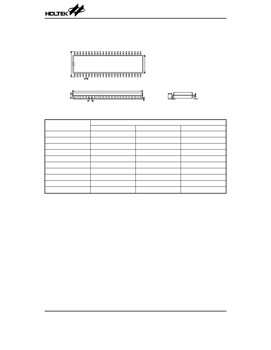
Package Information
48-pin SSOP (300mil) Outline Dimensions
Symbol
Dimensions in mil
Min.
Nom.
Max.
A
395
¾
420
B
291
¾
299
C
8
¾
12
C
¢
613
¾
637
D
85
¾
99
E
¾
25
¾
F
4
¾
10
G
25
¾
35
H
4
¾
12
a
0
°
¾
8
°
HT48R70A-1/HT48C70-1
Rev. 1.60
36
June 9, 2004
4 8
1
2 5
2 4
A
B
C
D
F
C '
G
H
a
E
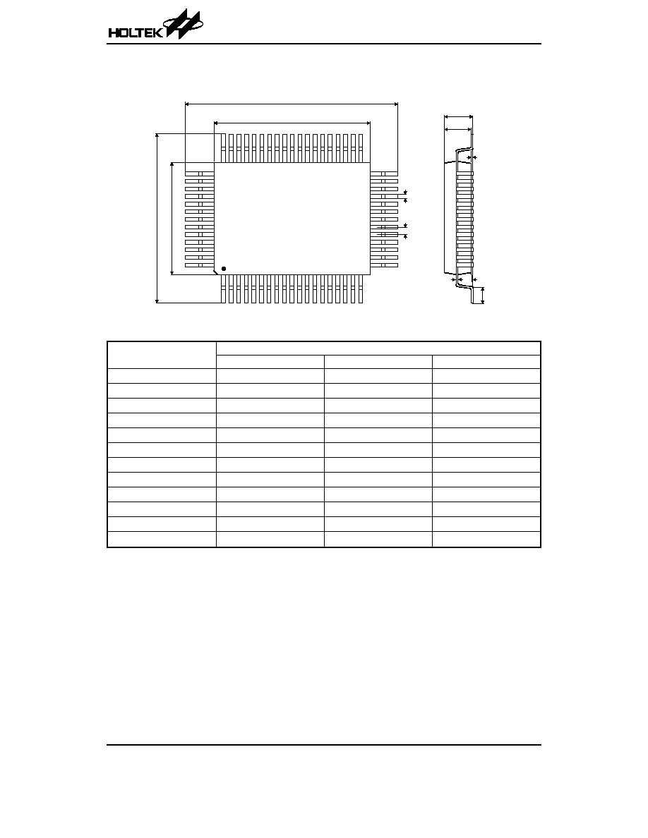
64-pin QFP (14
´20) Outline Dimensions
Symbol
Dimensions in mm
Min.
Nom.
Max.
A
18.80
¾
19.20
B
13.90
¾
14.10
C
24.80
¾
25.20
D
19.90
¾
20.10
E
¾
1
¾
F
¾
0.40
¾
G
2.50
¾
3.10
H
¾
¾
3.40
I
¾
0.10
¾
J
1.15
¾
1.45
K
0.10
¾
0.20
a
0
°
¾
7
°
HT48R70A-1/HT48C70-1
Rev. 1.60
37
June 9, 2004
5 1
5 2
6 4
1
2 0
3 2
3 3
1 9
A
B
C
D
E
F
G
H
I
J
K
a
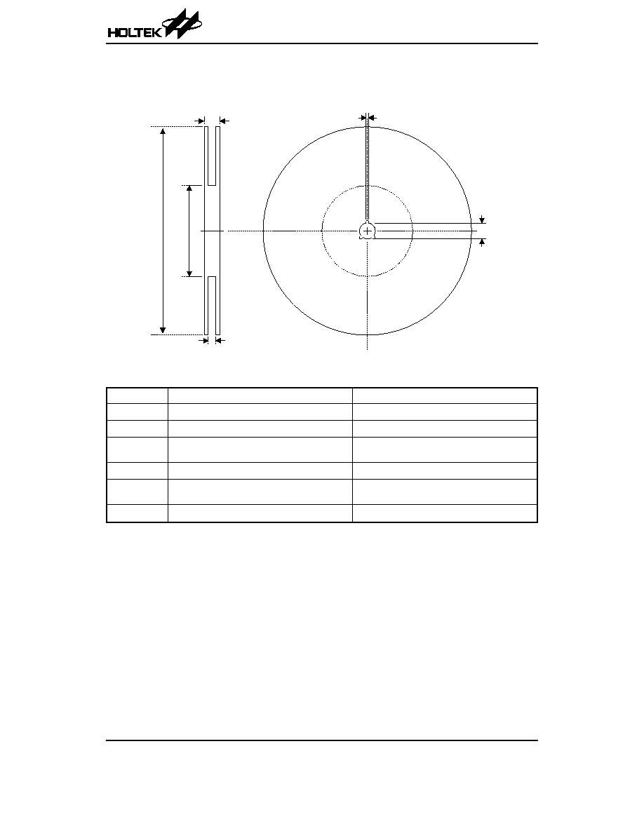
Product Tape and Reel Specifications
Reel Dimensions
SSOP 48W
Symbol
Description
Dimensions in mm
A
Reel Outer Diameter
330
±1.0
B
Reel Inner Diameter
100
±0.1
C
Spindle Hole Diameter
13.0+0.5
-0.2
D
Key Slit Width
2.0
±0.5
T1
Space Between Flange
32.2+0.3
-0.2
T2
Reel Thickness
38.2
±0.2
HT48R70A-1/HT48C70-1
Rev. 1.60
38
June 9, 2004
A
C
B
T 1
T 2
D
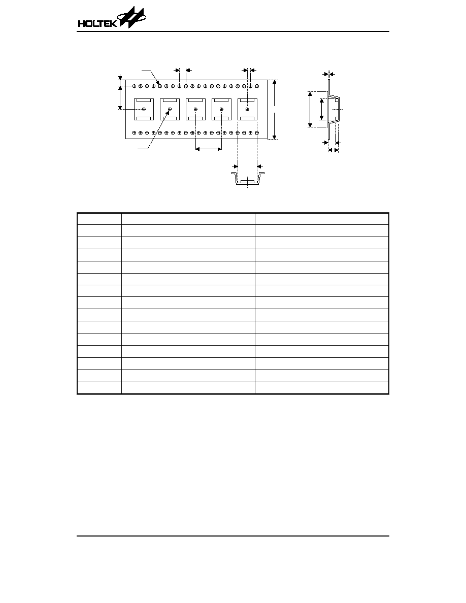
Carrier Tape Dimensions
SSOP 48W
Symbol
Description
Dimensions in mm
W
Carrier Tape Width
32.0
±0.3
P
Cavity Pitch
16.0
±0.1
E
Perforation Position
1.75
±0.1
F
Cavity to Perforation (Width Direction)
14.2
±0.1
D
Perforation Diameter
2.0 Min.
D1
Cavity Hole Diameter
1.5+0.25
P0
Perforation Pitch
4.0
±0.1
P1
Cavity to Perforation (Length Direction)
2.0
±0.1
A0
Cavity Length
12.0
±0.1
B0
Cavity Width
16.20
±0.1
K1
Cavity Depth
2.4
±0.1
K2
Cavity Depth
3.2
±0.1
t
Carrier Tape Thickness
0.35
±0.05
C
Cover Tape Width
25.5
HT48R70A-1/HT48C70-1
Rev. 1.60
39
June 9, 2004
P
D 1
P 1
P 0
D
E
F
t
K 2
B 0
A 0
W
K 1
C

HT48R70A-1/HT48C70-1
Rev. 1.60
40
June 9, 2004
Copyright
Ó 2004 by HOLTEK SEMICONDUCTOR INC.
The information appearing in this Data Sheet is believed to be accurate at the time of publication. However, Holtek as-
sumes no responsibility arising from the use of the specifications described. The applications mentioned herein are used
solely for the purpose of illustration and Holtek makes no warranty or representation that such applications will be suitable
without further modification, nor recommends the use of its products for application that may present a risk to human life
due to malfunction or otherwise. Holtek
¢s products are not authorized for use as critical components in life support devices
or systems. Holtek reserves the right to alter its products without prior notification. For the most up-to-date information,
please visit our web site at http://www.holtek.com.tw.
Holtek Semiconductor Inc. (Headquarters)
No.3, Creation Rd. II, Science Park, Hsinchu, Taiwan
Tel: 886-3-563-1999
Fax: 886-3-563-1189
http://www.holtek.com.tw
Holtek Semiconductor Inc. (Taipei Sales Office)
4F-2, No. 3-2, YuanQu St., Nankang Software Park, Taipei 115, Taiwan
Tel: 886-2-2655-7070
Fax: 886-2-2655-7373
Fax: 886-2-2655-7383 (International sales hotline)
Holtek Semiconductor Inc. (Shanghai Sales Office)
7th Floor, Building 2, No.889, Yi Shan Rd., Shanghai, China 200233
Tel: 021-6485-5560
Fax: 021-6485-0313
http://www.holtek.com.cn
Holtek Semiconductor Inc. (Shenzhen Sales Office)
43F, SEG Plaza, Shen Nan Zhong Road, Shenzhen, China 518031
Tel:0755-83465589
Fax:0755-83465590
ISDN : 0755-8346559
Holtek Semiconductor Inc. (Beijing Sales Office)
Suite 1721, Jinyu Tower, A129 West Xuan Wu Men Street, Xicheng District, Beijing, China 100031
Tel:010-66410030, 66417751, 66417752
Fax:010-66410125
Holmate Semiconductor, Inc. (North America Sales Office)
46712 Fremont Blvd., Fremont, CA 94538
Tel: 510-252-9880
Fax: 510-252-9885
http://www.holmate.com
Document Outline
- þÿ
- þÿ
- þÿ
- þÿ
- þÿ
- þÿ
- þÿ
- þÿ
- þÿ
- þÿ
- þÿ
- þÿ
- þÿ
- þÿ
- þÿ