 | –≠–ª–µ–∫—Ç—Ä–æ–Ω–Ω—ã–π –∫–æ–º–ø–æ–Ω–µ–Ω—Ç: HT49CV5 | –°–∫–∞—á–∞—Ç—å:  PDF PDF  ZIP ZIP |
Document Outline
- ˛ˇ
- ˛ˇ
- ˛ˇ
- ˛ˇ
- ˛ˇ
- ˛ˇ
- ˛ˇ
- ˛ˇ
- ˛ˇ
- ˛ˇ
- ˛ˇ
- ˛ˇ
- ˛ˇ
- ˛ˇ

HT49RV5/HT49CV5
A/D With VFD Type 8-Bit MCU
Rev. 1.20
1
April 14, 2006
Features
∑
Operating voltage:
f
SYS
=4MHz: 2.2V~5.5V
f
SYS
=8MHz: 3.3V~5.5V
∑
20 bidirectional I/O lines (PA, PB, PC, PD)
∑
Two external interrupt inputs
∑
Two 16-bit programmable timer/event counters with
PFD (programmable frequency divider) function
∑
One 8-bit Remote Control Timer (RMT), pin-shared
with PC7
∑
Single channel serial interface
∑
VFD driver with 11
¥11 segments
(16-segment & 4-grid to 11-segment & 11-grid)
∑
4K
¥16 program memory
∑
192
¥8 data memory RAM
∑
Supports PFD for sound generation
∑
Real Time Clock (RTC)
∑
8-bit prescaler for RTC
∑
Watchdog Timer
∑
Buzzer output
∑
On-chip crystal, RC and 32768Hz crystal oscillator
∑
HALT function and wake-up feature reduce power
consumption
∑
8-level subroutine nesting
∑
4-channel 8-bit resolution A/D converter
∑
2-channel 8-bit PWM output shared with 2 I/O lines
∑
Low voltage reset function
∑
Bit manipulation instruction
∑
16-bit table read instruction
∑
Up to 0.5
ms instruction cycle with 8MHz system clock
∑
63 powerful instructions
∑
All instructions in 1 or 2 machine cycles
∑
56-pin SSOP package
General Description
The HT49RV5/HT49CV5 are 8-bit high performance
single chip MCUs. Their single cycle instruction and
2-stage pipeline architecture make them suitable for
high speed applications. As the devices include an VFD
driver they are suitable for use in products which require
a front panel for their operation such as DVDs, VCDs,
Mini-component audio systems, cassette decks, tuners,
CD players, other home appliances, etc.
Technical Document
∑
Tools Information
∑
FAQs
∑
Application Note
-
HA0077E HT49CVX Remote Control Receiver SWIP Design Note
-
HA0078E HT49CVX Display SWIP Design Note
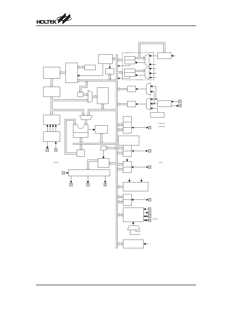
Block Diagram
HT49RV5/HT49CV5
Rev. 1.20
2
April 14, 2006
P r o g r a m
C o u n t e r
P r o g r a m
R O M
I n s t r u c t i o n
R e g i s t e r
I n s t r u c t i o n
D e c o d e r
T i m i n g
G e n e r a t i o n
O S C 2
O S C 4
O S C 1
R E S
V E E
I n t e r r u p t
C i r c u i t
I N T C
M P
M
U
X
M U X
D a t a
M e m o r y
A L U
S h i f t e r
S T A T U S
A C C
T M R 0 C
T M R 0
M
U
X
S t a c k
V F D
M e m o r y
B P
V F D D r i v e r
G r i d 0 ~
G r i d 5
S E G 1 1 / G r i d 1 0 ~
S E G 1 5 / G r i d 6
S E G 0 ~
S E G 1 0
T M R 1 C
T M R 1
M
U
X
P F D 0
P F D 1
f
S Y S
/ 4
f
S Y S
P r e s c a l e r
P D 6 / T M R 0
P A C
P A
P O R T A
P D
P D 0 / P W M 0 ~ P D 1 / P W M 1
P D 4 / I N T 0
P D 5 / I N T 1
P D 6 / T M R 0
P D 7 / T M R 1
P O R T B
P B
P B C
P B 0 / A N 0 ~ P B 3 / A N 3
P A 0 / B Z
P A 1 / B Z
P A 2
P A 3 / P F D
P A 4 ~ P A 7
4 - C h a n n e l
A / D C o n v e r t e r
H A L T
E N / D I S
L V R
3 2 7 6 8 H z
P D 7 / T M R 1
P C C
P C
P O R T C
P C 6
P C 7 / R M T
S e r i a l I n t e r f a c e
S D I
S D O
S C K
S C S
M U X
f
S Y S
/ 4
f
R T C O S C
8 - b i t R e m o t e
C o n t r o l T i m e r
R M T
V S S
O S C 3
V D D
P D C
P O R T D
P W M
M
U
X
W D T O S C
R T C O S C
O S C 3
O S C 4
W D T
R T C
f
S Y S
/ 4
M
U
X

Pin Assignment
Note:
Each V
DD
(V
SS
) pins must be connected to the power (ground) of the system.
Pin Description
Pin Name
I/O
Options
Description
PA0/BZ
PA1/BZ
PA2
PA3/PFD
PA4~PA7
I/O
Wake-up
Pull-high
Buzzer
PFD
Bidirectional 8-bit input/output port. Each bit can be configured as a wake-up
input by configuration option. Software instructions determine if the pin is a
CMOS output or Schmitt trigger input with or without pull-high resistor (deter-
mined by pull-high options: bit option). Pins PA0, PA1 and PA3 are
pin-shared with BZ, BZ and PFD, respectively.
PB0/AN0~
PB3/AN3
I/O
Pull-high
Bidirectional 4-bit input/output port. Software instructions determine if the pin
is a CMOS output or Schmitt trigger input with or without pull-high resistor
(determined by pull-high option: bit option) or A/D input. Once a PB line is se-
lected as an A/D input (by using software control), the I/O function and
pull-high resistor are disabled automatically.
PC6
PC7/RMT
I/O
Pull-high
Bidirectional 2-bit input/output port. Software instructions determine if the pin
is a CMOS output or Schmitt trigger input with or without pull-high resistor
(determined by pull-high option: bit option). RMT with wake-up function (both
rising and falling edge) and Schmitt trigger input with or without a pull-high re-
sistor (determined by pull-high option).
Note:The RMT is pin-shared with PC7. When PC7/RMT pin uses as the input
mode of RMT function , suggesting the user to set PC7 as input mode for
safety. And so that I/O function of PC7 will not influence the RMT input func-
tion.
HT49RV5/HT49CV5
Rev. 1.20
3
April 14, 2006
O S C 2
O S C 1
R E S
P A 0 / B Z
P A 1 / B Z
P A 2
P A 3 / P F D
P A 4
P A 5
P A 6
P A 7
P B 0 / A N 0
P B 1 / A N 1
P B 2 / A N 2
P B 3 / A N 3
V S S
P D 0 / P W M 0
P D 1 / P W M 1
P D 4 / I N T 0
P D 5 / I N T 1
P D 6 / T M R 0
P D 7 / T M R 1
V S S
P C 6
P C 7 / R M T
S E G 0
S E G 1
S E G 2
V D D
O S C 3
O S C 4
S D I
S D O
S C K
S C S
G R I D 0
G R I D 1
G R I D 2
G R I D 3
G R I D 4
G R I D 5
V D D
V E E
S E G 1 5 / G R I D 6
S E G 1 4 / G R I D 7
S E G 1 3 / G R I D 8
S E G 1 2 / G R I D 9
S E G 1 1 / G R I D 1 0
S E G 1 0
S E G 9
S E G 8
S E G 7
S E G 6
S E G 5
S E G 4
S E G 3
5 6
5 5
5 4
5 3
5 2
5 1
5 0
4 9
4 8
4 7
4 6
4 5
4 4
4 3
4 2
4 1
4 0
3 9
3 8
3 7
3 6
3 5
3 4
3 3
3 2
3 1
3 0
2 9
1
2
3
4
5
6
7
8
9
1 0
1 1
1 2
1 3
1 4
1 5
1 6
1 7
1 8
1 9
2 0
2 1
2 2
2 3
2 4
2 5
2 6
2 7
2 8
H T 4 9 R V 5 / H T 4 9 C V 5
5 6 S S O P - A
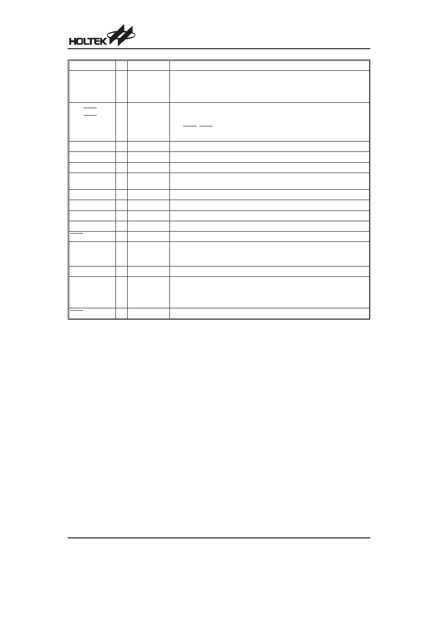
Pin Name
I/O
Options
Description
PD0/PWM0
PD1/PWM1
I/O
Pull-high
PWM
Bidirectional 2-bit input/output port. Software instructions determine if the pin
is a CMOS output or Schmitt trigger input with or without a pull-high resistor
(determined by pull-high option: bit option). PD0~PD1 are pin-shared with
PWM0~PWM1 (dependent on Mask options).
PD4/INT0
PD5/INT1
PD6/TMR0
PD7/TMR1
I/O
Pull-high
Bidirectional 4-bit input/output port. Software instructions determine if the pin
is a CMOS output or Schmitt trigger input with or without a pull-high resistor
(determined by pull-high option: bit option). Pins PD4~PD7 are pin-shared
with INT0, INT1, TMR0 & TMR1, respectively (determined by software con-
trol).
VSS
æ
æ
Negative power supply, ground
VEE
æ
æ
VFD Negative power supply
SEG0~SEG10
O
æ
High voltage segment output for VFD panel.
SEG11/Grid10~
SEG15/Grid6
O
æ
High voltage output for VFD panel. These pins are selectable for segment or
grid output.
Grid0~Grid5
O
æ
High voltage grid output for VFD panel.
SDI
I
æ
Serial interface serial data input
SDO
O
æ
Serial interface serial data output
SCK
I/O
æ
Serial interface serial clock input/output (initial
≤input≤).
SCS
I/O
æ
Serial interface chip select pin, output for master mode, input for slave mode.
OSC4
OSC3
O
I
RTC or
System Clock
Real time clock oscillators. OSC3 and OSC4 are connected to a 32768Hz
crystal oscillator for timing purposes or to a system clock source (depending
on the options). No built-in capacitor.
VDD
æ
æ
Positive power supply
OSC2
OSC1
O
I
Crystal or RC
OSC1 and OSC2 are connected to an RC network or a crystal (by options) for
the internal system clock. For RC operation, OSC2 is an output pin for 1/4
system clock. The system clock may come from the RTC oscillator. If the sys-
tem clock comes from RTCOSC, these two pins can be left floating.
RES
I
æ
Schmitt trigger reset input, active low
Absolute Maximum Ratings
Supply Voltage ...........................V
SS
-0.3V to V
SS
+6.0V
Storage Temperature ............................
-50∞C to 125∞C
Input Voltage..............................V
SS
-0.3V to V
DD
+0.3V
Operating Temperature...........................
-40∞C to 85∞C
Note: These are stress ratings only. Stresses exceeding the range specified under
≤Absolute Maximum Ratings≤ may
cause substantial damage to the device. Functional operation of this device at other conditions beyond those
listed in the specification is not implied and prolonged exposure to extreme conditions may affect device reliabil-
ity.
HT49RV5/HT49CV5
Rev. 1.20
4
April 14, 2006

D.C. Characteristics
Ta=25
∞C
Symbol
Parameter
Test Conditions
Min.
Typ.
Max.
Unit
V
DD
Conditions
V
DD
Operating Voltage
æ f
SYS
=4MHz
2.2
æ
5.5
V
æ f
SYS
=8MHz
3.3
æ
5.5
V
V
EE
VFD Supply Voltage
æ
æ
0
æ
V
DD
-30
V
I
DD1
Operating Current (Crystal OSC)
3V
No load, ADC off, VFD off,
f
SYS
=4MHz
æ
2.0
3.0
mA
5V
æ
5.0
8.0
mA
I
DD2
Operating Current (RC OSC)
3V
No load, ADC off, VFD off,
f
SYS
=4MHz
æ
1.8
2.7
mA
5V
æ
4.6
7.5
mA
I
DD3
Operating Current
(f
SYS
=32768Hz)
3V
No load, ADC off, VFD off
æ
1.2
2
mA
5V
æ
4
7
mA
I
DD4
Operating Current (Crystal OSC)
3V
No load, ADC off, VFD on,
f
SYS
=4MHz
æ
3.5
4.5
mA
5V
æ
7.5
12
mA
I
STB1
Standby Current (*f
S
=T1)
3V
No load, system HALT
VFD off at HALT
æ
æ
1
mA
5V
æ
æ
2
mA
I
STB2
Standby Current
(*f
S
=32768Hz OSC)
3V
No load, system HALT
VFD off at HALT
æ
4
10
mA
5V
æ
14
20
mA
V
IL1
Input Low Voltage for I/O Ports,
TMR and INT
3V
æ
0
æ
0.2V
DD
V
5V
V
IH1
Input High Voltage for I/O Ports,
TMR and INT
3V
æ
0.8V
DD
æ
V
DD
V
5V
V
IL2
Input Low Voltage (RES)
3V
æ
0
æ
0.4V
DD
V
5V
V
IH2
Input High Voltage (RES)
3V
æ
0.9V
DD
æ
V
DD
V
5V
I
OL
I/O Port Sink Current
3V
V
OL
=0.1V
DD
6
12
æ
mA
5V
10
25
æ
mA
I
OH1
I/O Port Source Current
3V
V
OH
=0.9V
DD
-2
-4
æ
mA
5V
-5
-8
æ
mA
I
OH2
Grid Source Current
5V
V
OH
=V
DD
-2V
-15
æ
æ
mA
I
OH3
Segment Source Current
5V
V
OH
=V
DD
-2V
-3
æ
æ
mA
R
PH
Pull-high Resistance of I/O Ports
and INT0, INT1
3V
æ
20
60
100
k
W
5V
æ
10
30
50
k
W
R
PL
VFD Driver Output Pull-low
Resistor
5V
æ
50
100
150
k
W
V
LVR
Low Voltage Reset Voltage
æ LVRenabled
2.7
3.0
3.3
V
V
AD
A/D Input Voltage
æ
æ
0
æ
V
DD
V
E
AD
A/D Conversion Error
3V
æ
æ
±0.5
±1
LSB
5V
I
ADC
Additional Power Consumption
if A/D Converter is Used
3V
No load
æ
1
2
mA
5V
æ
2
4
mA
Note:
≤*f
S
≤ Refer to WDT clock option
HT49RV5/HT49CV5
Rev. 1.20
5
April 14, 2006