 | –≠–ª–µ–∫—Ç—Ä–æ–Ω–Ω—ã–π –∫–æ–º–ø–æ–Ω–µ–Ω—Ç: HT6207 | –°–∫–∞—á–∞—Ç—å:  PDF PDF  ZIP ZIP |
Document Outline
- ˛ˇ
- ˛ˇ
- ˛ˇ
- ˛ˇ
- ˛ˇ
- ˛ˇ
- ˛ˇ
- ˛ˇ
- ˛ˇ
- ˛ˇ
- ˛ˇ
HT600/680/6207
3
18
Series of Encoders
Selection Table
Function Address
No.
Address/
Data No.
Data
No.
Dummy
Code No.
Oscillator
Trigger
Package
Part No.
HT600
9
5
0
4
RC oscillator
TE
20 DIP/SOP
HT680
8
4
0
6
RC oscillator
TE
18 DIP/SOP
HT6207
10
0
4
4
RC oscillator
D12~D15
20 DIP/SOP
Note: Address/Data represents addressable pins or data according to the decoder requirements.
1
April 24, 2000
General Description
The 3
18
encoders are a series of CMOS LSIs for
remote control system applications. They are
capable of encoding 18 bits of information
which consists of N address bits and 18-N data
bits. Each address/data input is externally
trinary programmable if bonded out. It is other-
wise set floating internally. Various packages of
the 3
18
encoders offer flexible combinations of
programmable address/data to meet various
application needs. The programmable ad-
dress/data is transmitted together with the
header bits via an RF or an infrared transmis-
sion medium upon receipt of a trigger signal.
The capability to select a TE trigger type or a
DATA trigger type further enhances the appli-
cation flexibility of the 3
18
series of encoders.
Features
∑
Operating voltage: 2.4V~12V
∑
Low power and high noise immunity CMOS
technology
∑
Low standby current
∑
Three words transmission
∑
Built-in oscillator needs only 5% resistor
∑
Easy interface with an RF or infrared trans-
mission media
∑
Minimal external components
∑
Package information: refer to Selection
Table
Applications
∑
Burglar alarm system
∑
Smoke and fire alarm system
∑
Garage door controllers
∑
Car door controllers
∑
Car alarm system
∑
Security system
∑
Cordless telephones
∑
Other remote control systems
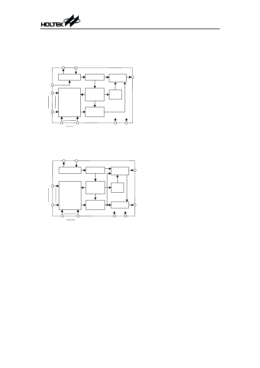
Block Diagram
TE trigger
HT600/HT680
DATA trigger
HT6207
Note: The address/data pins are available in various combinations.
HT600/680/6207
2
April 24, 2000
O s c i l l a t o r
∏ 3 3 D i v i d e r
O S C 1
O S C 2
V D D
V S S
1 8
T r a n s m i s s i o n
G a t e C i r c u i t
∏ 1 8 C o u n t e r
& 1 o f 1 8
D e c o d e r
T r i n a r y
D e t e c t o r
A 0
A 9
A D 1 7
D O U T
D a t a S e l e c t
& B u f f e r
S y n c .
C i r c u i t
T E
A D 1 0
O s c i l l a t o r
∏ 3 3 D i v i d e r
O S C 1
O S C 2
V D D
V S S
1 8
T r a n s m i s s i o n
G a t e C i r c u i t
∏ 1 8 C o u n t e r
& 1 o f 1 8
D e c o d e r
T r i n a r y
D e t e c t o r
D O U T
D a t a S e l e c t
& B u f f e r
S y n c .
C i r c u i t
L E D C i r c u i t
L E D
A 0
A 1 1
D 1 7
D 1 2
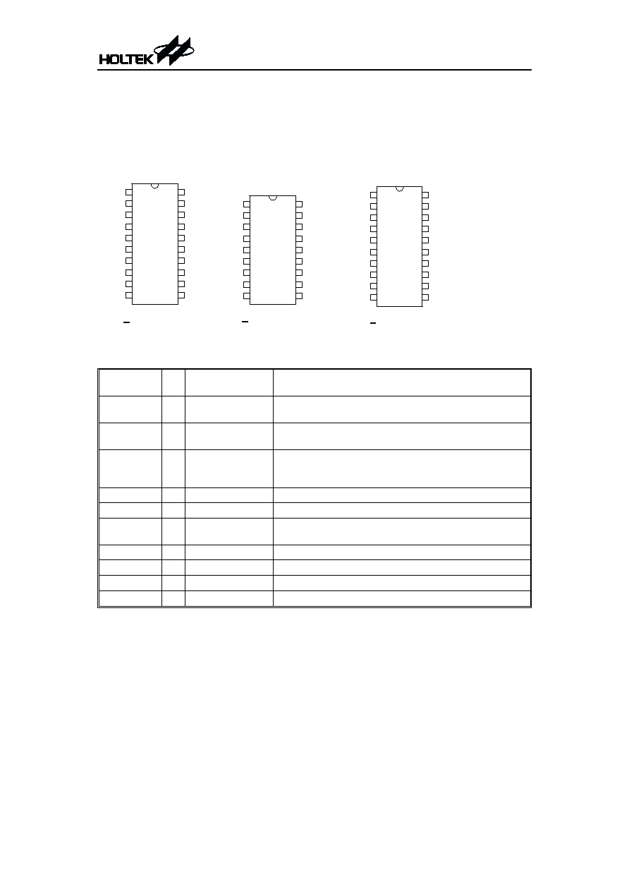
Pin Assignment
Pin Description
Pin Name I/O
Internal
Connection
Description
A0~A11
I
TRANSMISSION
GATE
Input pins for address A0~A11 setting
They can be externally set to VDD, VSS, or left open.
AD10~AD17
I
TRANSMISSION
GATE
Input pins for address/data (AD10~AD17) setting
They can be externally set to VDD, VSS, or left open.
D12~D15
I
CMOS IN
Pull-low
Input pins for data (D12~D15) setting and transmission
enable (active high)
They an be externally set to VDD or left open (see Note).
DOUT
O
CMOS OUT
Encoder data serial transmission output
LED
O
NMOS OUT
LED transmission enable indicator
TE
I
CMOS IN
Pull-low
Transmission enable, active high (see Note).
OSC1
I
OSCILLATOR
Oscillator input pin
OSC2
O
OSCILLATOR
Oscillator output pin
VSS
æ
æ
Negative power supply, ground
VDD
æ
æ
Positive power supply
Note: D12~D15 are data input and transmission enable pins of the HT6207.
TE is the transmission enable pin of the HT600/HT680.
HT600/680/6207
3
April 24, 2000
9 - A d d r e s s
5 - A d d r e s s / D a t a
H T 6 0 0
2 0 D I P / S O P
T E t r i g g e r t y p e
8 - A d d r e s s
4 - A d d r e s s / D a t a
H T 6 8 0
1 8 D I P / S O P
V D D
A 9
A 8
A 7
A 6
A 3
A 2
A 1
A 0
1 8
1 7
1 6
1 5
1 4
1 3
1 2
1 1
1 0
1
2
3
4
5
6
7
8
9
A D 1 1
A D 1 2
A D 1 4
A D 1 5
D O U T
T E
O S C 2
O S C 1
V S S
V D D
A 9
A 8
A 7
A 6
A 4
A 3
A 2
A 1
A 0
2 0
1 9
1 8
1 7
1 6
1 5
1 4
1 3
1 2
1 1
1
2
3
4
5
6
7
8
9
1 0
A D 1 1
A D 1 2
A D 1 3
A D 1 4
A D 1 5
D O U T
T E
O S C 2
O S C 1
V S S
D A T A t r i g g e r t y p e
1 0 - A d d r e s s
4 - D a t a
H T 6 2 0 7
2 0 D I P / S O P
A 1 1
D 1 2
D 1 3
D 1 4
D 1 5
D O U T
L E D
O S C 2
O S C 1
V S S
1
2
3
4
5
6
7
8
9
1 0
2 0
1 9
1 8
1 7
1 6
1 5
1 4
1 3
1 2
1 1
V D D
A 9
A 8
A 7
A 6
A 4
A 3
A 2
A 1
A 0
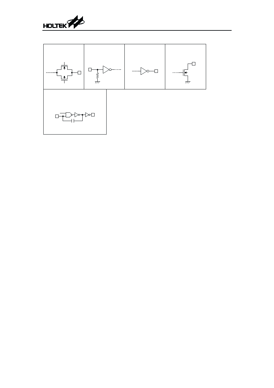
Approximate internal connections
Absolute Maximum Ratings
Supply Voltage...............................-0.3V to 13V
Storage Temperature.................-50∞C to 125∞C
Input Voltage....................V
SS
-0.3 to V
DD
+0.3V
Operating Temperature ..............-20∞C to 75∞C
Note: These are stress ratings only. Stresses exceeding the range specified under ≤Absolute Maxi-
mum Ratings≤ may cause substantial damage to the device. Functional operation of this de-
vice at other conditions beyond those listed in the specification is not implied and prolonged
exposure to extreme conditions may affect device reliability.
HT600/680/6207
4
April 24, 2000
T R A N S M I S S I O N
G A T E
C M O S I N
P u l l - l o w
C M O S O U T
O S C I L L A T O R
O S C 1
O S C 2
E N
N M O S O U T
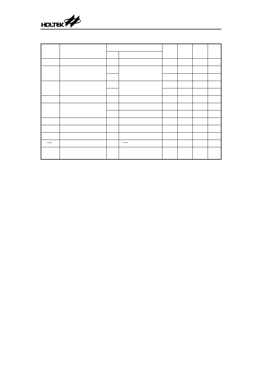
Electrical Characteristics
Ta=25∞C
Symbol
Parameter
Test Conditions
Min.
Typ.
Max. Unit
V
DD
Conditions
V
DD
Operating Voltage
æ
æ
2.4
æ
12
V
I
STB
Standby Current
3V
Oscillator stops
æ
0.1
1
mA
12V
æ
2
4
mA
I
DD
Operating Current
5V No load
f
OSC
=100kHz
æ
250
500
mA
12V
æ
1200
2400
mA
I
LED
LED Sink Current
5V V
LED
=0.5V
1.5
3
æ
mA
I
DOUT
Output Drive Current
5V V
OH
=0.9V
DD
(Source)
-0.6
-1.2
æ
mA
5V V
OL
=0.1V
DD
(Sink)
0.6
1.2
æ
mA
V
IH
≤H≤ Input Voltage
æ
æ
0.8V
DD
æ
V
DD
V
V
IL
≤L≤ Input Voltage
æ
æ
0
æ
0.2V
DD
V
f
OSC
Oscillator Frequency
10V R
OSC
=330kW
æ
100
æ
kHz
R
TE
TE Pull-low Resistance
5V
V
TE
=5V
æ
1.5
3
MW
R
DATA
D12~D17 Pull-low
Resistance
5V V
DATA
=5V
æ
1.5
3
MW
HT600/680/6207
5
April 24, 2000