Document Outline
- ˛ˇ
- ˛ˇ
- ˛ˇ
- ˛ˇ
- ˛ˇ
- ˛ˇ
- ˛ˇ
- ˛ˇ
- ˛ˇ
- ˛ˇ
- ˛ˇ
- ˛ˇ
- ˛ˇ
- ˛ˇ
- ˛ˇ
HT6240-002
Infrared Remote Encoder
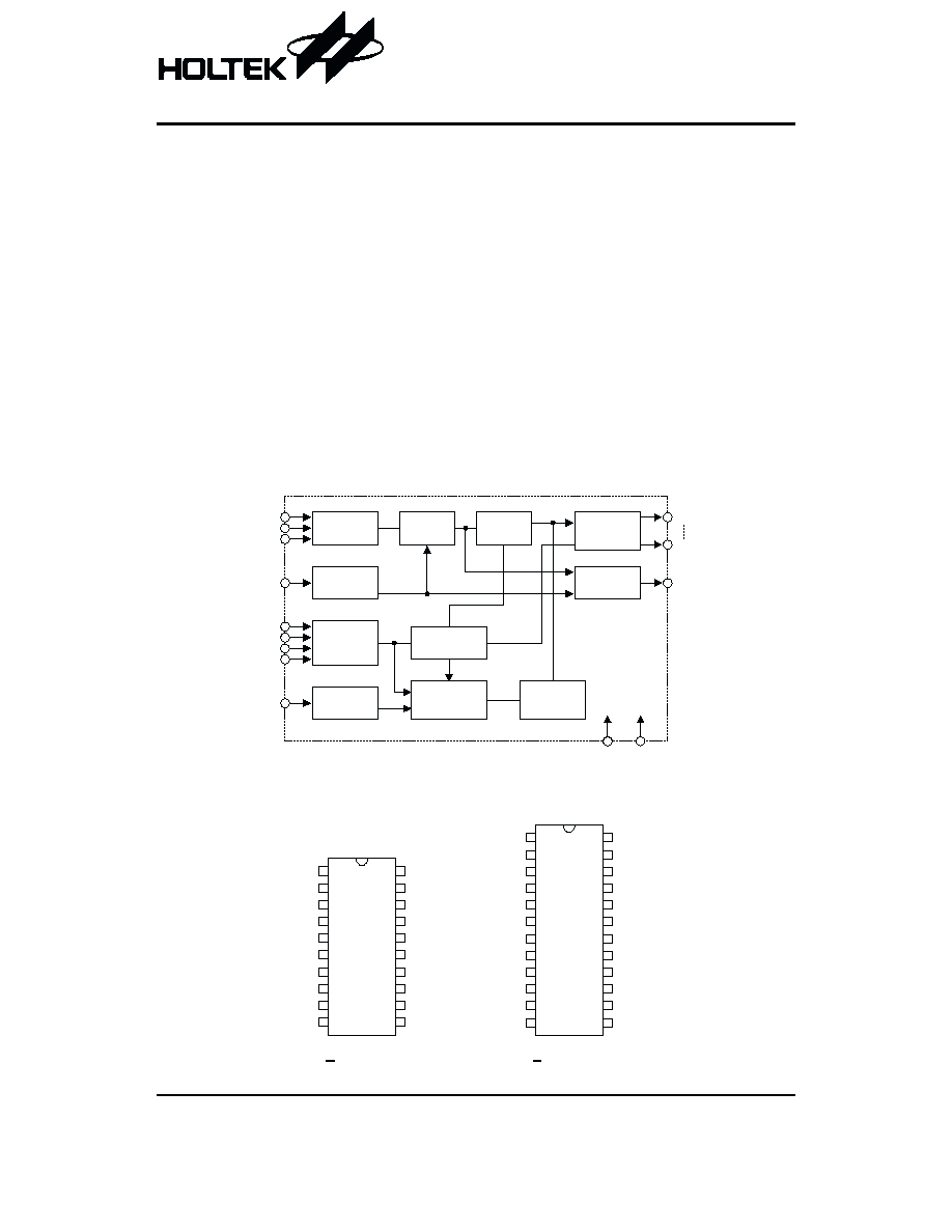
Block Diagram
Pin Assignment
Rev. 1.30
1
November 6, 2002
Features
∑
Operating voltage: 2.2V~3.6V
∑
Low power consumption
∑
Few external parts
∑
20/24-pin SOP package
Applications
∑
Television and video cassette recorder
controllers
∑
Garage door controllers
∑
Car door controllers
∑
Security systems
∑
Other remote control systems
General Description
HT6240-002 is designed as infrared remote encoders,
usually applied to TV systems. The 4
¥8 key matrix input
and the extension bit input can transmit a max. of 256 in-
structions. HT6240-002 have two different packages:
20-pin SOP and 24-pin SOP.
3 ¥ 2
D u t y 1 / 3
2
1 0 ¥ 2
D i v i d e r
8
T E S T
M O D E
O S C
T E S T
V D D
V S S
P R B
O S C I
O S C O
C o n t r o l
U n i t
C u s t o m C o d e
& D A T A C o d e
L a t c h
K e y S c a n
D r i v e r
D e c o d e r
O u t p u t
S t a g e
O . 0
O . 7
I E - K E Y
E n c o d e r
8 - B i t S h i f t
R e g i s t e r
D A T A
I E 0
I E 1
I E 2
I E 3
P a r a l l e l t o
S e r i a l
C o n v e r t e r
C T
2 4
2 3
2 2
2 1
2 0
1 9
1 8
1 7
1 6
1 5
1 4
1 3
1
2
3
4
5
6
7
8
9
1 0
1 1
1 2
2 0
1 9
1 8
1 7
1 6
1 5
1 4
1 3
1 2
1 1
1
2
3
4
5
6
7
8
9
1 0
V D D
C T
O . 0
O . 1
O . 2
O . 3
O . 4
O . 5
O . 6
O . 7
V S S
T E S T
P R B
O S C I
O S C O
D A T A
I E 0
I E 1
I E 2
I E 3
H T 6 2 4 0 - 0 0 2
2 0 S O P - A
V D D
C T
O . 0
O . 1
O . 2
O . 3
O . 4
O . 5
O . 6
O . 7
N C
N C
V S S
T E S T
P R B
O S C I
O S C O
D A T A
I E 0
I E 1
I E 2
I E 3
N C
N C
H T 6 2 4 0 - 0 0 2
2 4 S O P - A
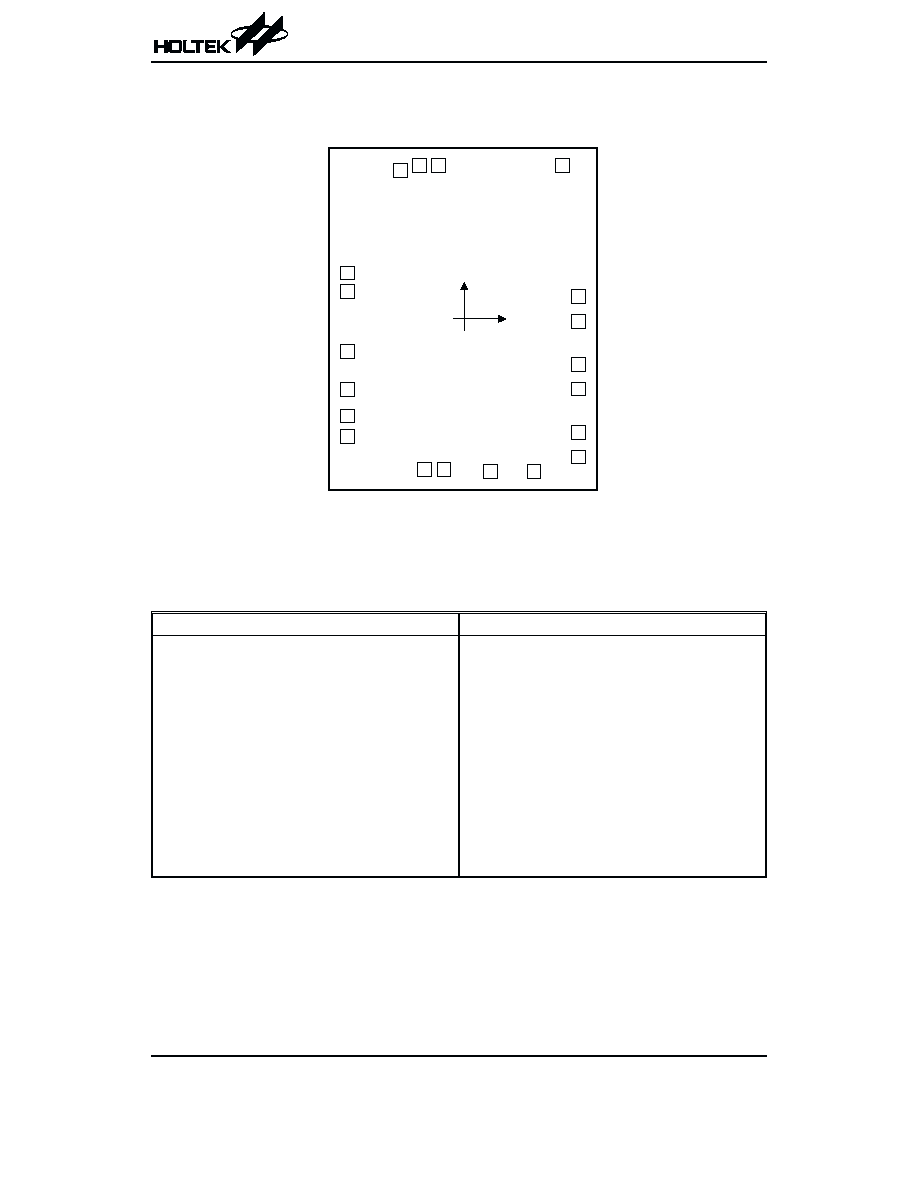
Pad Assignment
Chip size: 92
¥ 118 mil
2
* The IC substrate should be connected to VDD in the PCB layout artwork.
Pad Coordinates
Unit: mil
Pad No.
X
Y
Pad No.
X
Y
1
-40.88
16.11
11
40.12
-48.32
2
-40.88
9.48
12
40.12
-39.74
3
-40.88
-11.56
13
40.12
-24.57
4
-40.88
-24.78
14
40.12
-15.98
5
-40.88
-34.04
15
40.12
-0.81
6
-40.88
-41.18
16
40.12
7.78
7
-13.77
-52.78
17
34.47
53.59
8
-7.14
-52.78
18
-8.97
53.59
9
9.22
-53.55
19
-15.60
53.59
10
24.40
-53.55
20
-22.23
52.02
HT6240-002
Rev. 1.30
2
November 6, 2002
1
1 1
2
1 2
3
1 3
4
1 4
5
1 5
6
1 6
7
1 7
8
1 8
9
1 9
1 0
2 0
P R B
O S C I
O S C O
D A T E
I E 0
I E 1
I
E
2
I
E
3
O
.
7
O
.
6
O . 5
O . 4
O . 3
O . 1
O . 2
O . 0
C
T
V
D
D
V
S
S
T
E
S
T
( 0 , 0 )
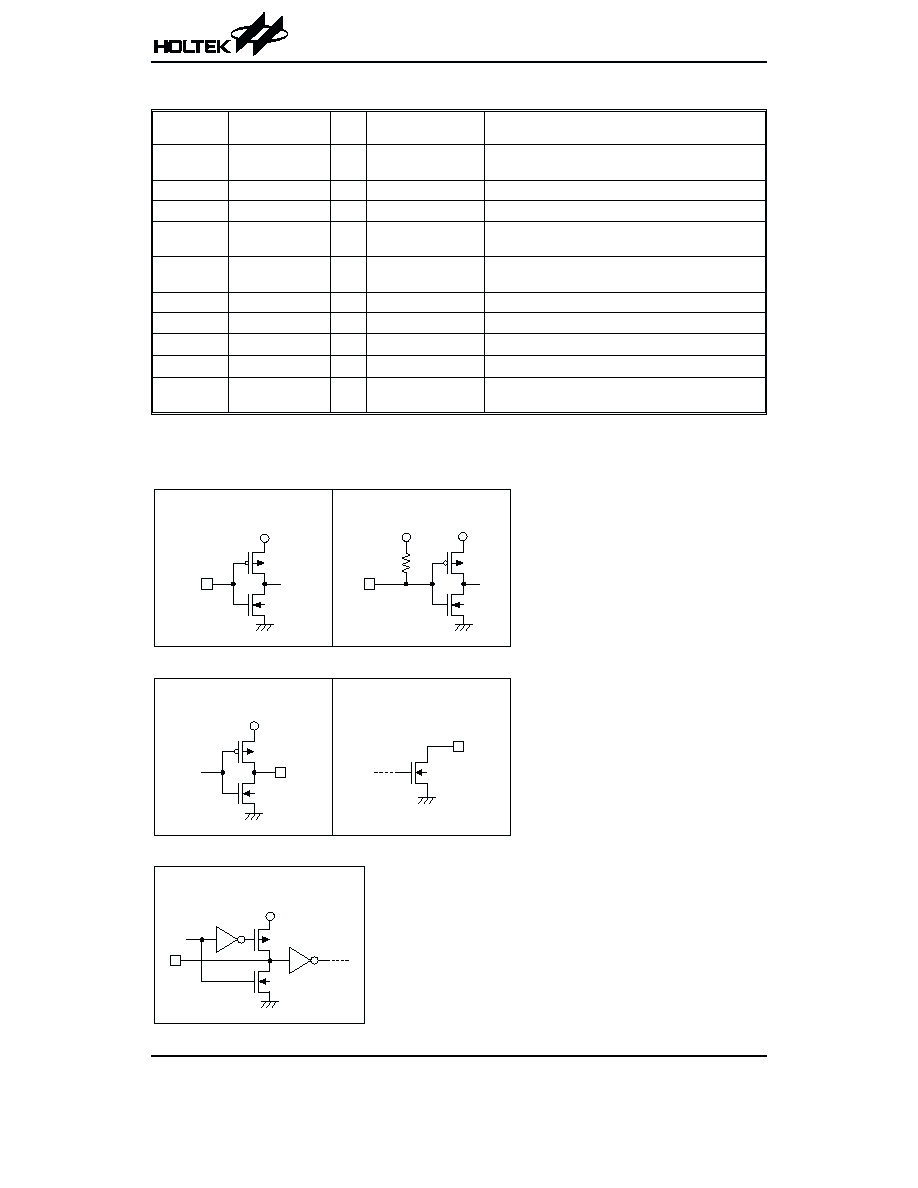
Pad Description
Pad No.
Pad Name
I/O
Internal
Connection
Description
1
PRB
I
CMOS
Pull-high
Power on reset
2
OSCI
I
CMOS
Oscillator input
3
OSCO
O
CMOS
Oscillator output
4
DATA
I/O
CMOS, NMOS
Pull-high
Detect custom code and extended code
5~8
IE0~IE3
I
CMOS
Pull-high
Detect input from key matrix
9~16
OF7~OF0
O
NMOS
Drive for key scan
17
CT
O
CMOS
Generates output transmission code
18
VDD
æ
æ
Positive power supply
19
VSS
æ
æ
Negative power supply
20
TEST
I
CMOS
TEST=Low normal mode
TEST=High test mode
Approximate internal connection circuits
HT6240-002
Rev. 1.30
3
November 6, 2002
P i n : T E S T , O S C I
P i n : P R B , I E 0 ~ I E 3
I n p u t t e r m i n a l
V
D D
V
D D
V
D D
P i n : O S C O , C T
P i n : O . 0 ~ O . 7
O u t p u t t e r m i n a l
V
D D
P i n : D A T A
B i d i r e c t i o n a l t e r m i n a l
V
D D

Absolute Maximum Ratings
Supply Voltage .........................................
-0.3V to 5.2V
Input Voltage ..................................V
SS
-0.3 to V
DD
+0.3
Output Voltage..............................................V
SS
to V
DD
Storage Temperature ............................
-40∞C to 125∞C
Operating Temperature ...........................
-20∞C to 70∞C
Note: These are stress ratings only. Stresses exceeding the range specified under
≤Absolute Maximum Ratings≤ may
cause substantial damage to the device. Functional operation of this device at other conditions beyond those
listed in the specification is not implied and prolonged exposure to extreme conditions may affect device reliabil-
ity.
Recommended Operating Condition
Ta=
-20∞C~70∞C, unless otherwise noted
Symbol
Parameter
Test Conditions
Min.
Typ.
Max.
Unit
V
DD
Conditions
V
DD
Supply Voltage
æ
æ
2.2
æ
3.6
V
V
IH
High-level Input Voltage IE0~IE3, DATA
3V
æ
2.4V
3V
3V
V
High-level Voltage PRB
3V
æ
2.1V
3V
3V
V
IL
Low-level Input Voltage IE0~IE3, DATA
3V
æ
0
0
1.2V
V
Low-level Input Voltage PRB
3V
æ
0
0
0.9V
f
OSC
Clock Oscillating Frequency
3V
æ
æ
455
æ
kHz
Electric Characteristics
Ta=25
∞C, V
DD
=3V, V
SS
=0V, unless otherwise noted
Symbol
Parameter
Test Conditions
Limits
Unit
V
DD
Conditions
Min.
Typ.
Max.
V
DD
Supply Voltage
æ
f
OSC
=455kHz,
Ta=
-20∞C~70∞C
2.2
æ
3.6
V
I
DD
Supply Current (during operation)
3V
f
OSC
=455kHz
æ
0.1
0.3
mA
I
DD
Supply Current (while not in operation)
3V
æ
æ
æ
1
mA
I
OH
High-level Output Current CT
3V
V
OH
=2V
-5
-10
æ
mA
I
OL
Low-level Output Current CT
3V
V
OL
=0.9V
0.3
0.8
æ
mA
Low-level Output Current DATA
3V
V
OL
=0.9V
1
4
æ
Low-level Output Current OF0~OF7
3V
V
OL
=0.9V
1
4
æ
R
I
Pull-up Resistance PRB
3V
æ
æ
80
æ
k
W
Pull-up Resistance DATA
3V
æ
æ
70
æ
Pull-up Resistance E0~E3
3V
æ
æ
70
æ
HT6240-002
Rev. 1.30
4
November 6, 2002

HT6240-002
Rev. 1.30
5
November 6, 2002
Functional Description
Key operation
The input pins (IE0~IE3) and the output pins
(OF0~OF7) constitute a max. of 4
¥8 key matrix which is
also called standard key. The extended key is formed by
input pin DATA and the scan output (OF5~OF7). The
4
¥8 key matrix and the extended key can transmit a
max. of 256 instruction.
CT maintains
≤L≤ and no transmission code is gener-
ated when two or more keys in standard key are
pressed.
Table 1 shows the relationship between the key matrix
and the transmission code.
Table 1
Transmission Code
Key Input
D1
D0
IE0
0
0
IE1
0
1
IE2
1
0
IE3
1
1
Transmission Code
Scan Output
D4
D3
D2
OF0
0
0
0
OF1
0
0
1
OF2
0
1
0
OF3
0
1
1
OF4
1
0
0
OF5
1
0
1
OF6
1
1
0
OF7
1
1
1
Transmission Code
DATA Input
D7
D6
D5
OF5
æ
æ
1
OF6
æ
1
æ
OF7
1
æ
æ
Custom code
The custom code is made up of input pin DATA and scan
output OF0~OF4. It has 8 bits (C0~C7); the lower 3 bits
of the custom code (C5, C6 and C7) are fixed as
≤0≤.
Fig. 1 shows an example of custom code selection.
Extended bit
The extended bit is formed by input pin DATA and the
scan output (OF5~OF7). Fig. 2 shows an example of ex-
tended bit selection.
Clock oscillating circuit
HT6240 has built-in feedback resistor and CMOS in-
verter, so a ceramic resonator can connect between the
oscillator circuit input pin (OSCI) and the output pin
(OSCO), (see Fig. 3).
When the ceramic resonator is set to 455kHz, the carrier
can be set 38kHz.
D A T A
O . 5 O . 6 O . 7
D A T A c o d e
S W = O N
S W = O . .
D 5
1
1
D 6
1
0
D 7
0
0
S W
Fig. 2
D A T A
O . 0 O . 1 O . 2 O . 3 O . 4
C u s t o m c o d e C 0
1
C 1
1
C 2
0
C 3
0
C 4
1
C 5
0
C 6
0
C 7
0
Fig. 1