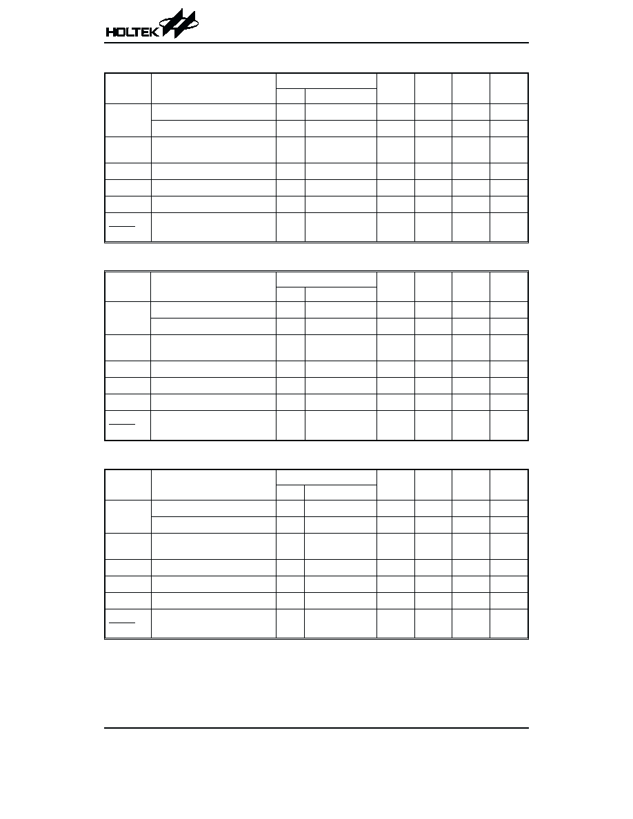
HT70XX
Voltage Detector
Selection Table
Part No.
Detectable Voltage
Hysteresis Width
Tolerance
HT7022A
2.2V
0.11V
±5%
HT7024A
2.4V
0.12V
±5%
HT7027A
2.7V
0.135V
±5%
HT7033A
3.3V
0.165V
±5%
HT7039A
3.9V
0.195V
±5%
HT7044A
4.4V
0.22V
±5%
HT7050A
5.0V
0.25V
±5%
HT7070A
7.0V
0.35V
±5%
Note:
The output type selection codes are:
NMOS open drain normal open, active low
For example: The HT7070A is a 7.0V, NMOS open drain active low output
Output type selection table
V
DD
V
DD
>V
DET
(+)
V
DD
£V
DET
(
-)
Type
V
OUT
A
Hi-Z
VSS
Rev. 1.60
1
January 14, 2003
General Description
The HT70XX series is a set of three-terminal low power
voltage detectors implemented in CMOS technology.
Each voltage detector in the series detects a particular
fixed voltage ranging from 2.2V to 7V. The voltage de-
tectors consist of a high-precision and low power con-
sumption standard voltage source, a comparator,
hysteresis circuit, and an output driver. CMOS technol-
ogy ensures low power consumption.
Although designed primarily as fixed voltage detectors,
these devices can be used with external components to
detect user specified threshold voltages (NMOS open
drain type only).
Features
∑
Low power consumption
∑
Low temperature coefficient
∑
Built-in high-stability reference source
∑
Built-in hysteresis characteristic
∑
TO-92 & SOT-89 package
Applications
∑
Battery checkers
∑
Level selectors
∑
Power failure detectors
∑
Microcomputer reset
∑
Battery memory backup
∑
Non-volatile RAM signal storage protectors
Pad Assignment
HT70XX (except HT7022A)
Chip size: 1317
¥ 1158 (mm)
2
* The IC substrate should be connected to VDD in the
PCB layout artwork.
HT7022A only
Chip size: 2032
¥ 1321 (mm)
2
* The IC substrate should be connected to VDD in the
PCB layout artwork.
Absolute Maximum Ratings
Supply Voltage, except HT7022A ..................................................................................................V
SS
-0.3V to V
SS
+26V
Supply Voltage, HT7022A only ....................................................................................................................
-0.3V to 13V
Output Voltage ...........................V
SS
-0.3V to V
DD
+0.3V
Output Current......................................................50mA
Storage Temperature ............................
-50∞C to 125∞C
Power Consumption ..........................................200mW
Operating Temperature ...............................0
∞C to 70∞C
Note: These are stress ratings only. Stresses exceeding the range specified under
≤Absolute Maximum Ratings≤ may
cause substantial damage to the device. Functional operation of this device at other conditions beyond those
listed in the specification is not implied and prolonged exposure to extreme conditions may affect device reliabil-
ity.
HT70XX
Rev. 1.60
3
January 14, 2003
1
2
3
( 0 , 0 )
O
U
T
V
D
D
V
S
S
1
2
3
( 0 , 0 )
V
O
U
T
V
I
N
G
N
D
Pad Coordinates
HT70XX (except HT7022A)
Unit:
mm
Pad No.
X
Y
1
-483.30
-379.50
2
-234.60
-399.50
3
443.90
-386.00
HT7022A only
Unit:
mm
Pad No.
X
Y
1
-434.34
394.97
2
120.65
461.01
3
774.70
412.75