
HT73XX
Low Power Consumption LDO
Selection Table
Part No.
Output Voltage
Tolerance
Package
Marking
HT7318
1.8V
±3%
TO-92-A
TO-92-B
SOT-89-A
73XX-A (for TO-92-A)
73XX-B (for TO-92-B)
73XX-A (for SOT-89)
HT7325
2.5V
±3%
HT7327
2.7V
±3%
HT7330
3.0V
±3%
HT7333
3.3V
±3%
HT7335
3.5V
±3%
HT7350
5.0V
±3%
Note:
≤XX≤ stands for output voltages
Rev. 1.10
1
July 30, 2004
Features
∑
Ultra low quiescent current: 4
mA (typ.)
∑
High input voltage (up to 12V)
∑
Output voltage:
1.8V, 2.5V, 2.7V, 3.0V, 3.3V, 3.5V, 5.0V
∑
Output voltage accuracy: tolerance
±3%
∑
Maximum output current: 250mA
∑
Low dropout voltage
∑
Low temperature coefficient
∑
TO-92, SOT-89 package
Applications
∑
Battery-powered equipment
∑
Voltage regulator for microprocessor
∑
Voltage regulator for LAN cards
∑
Wireless Communication equipment
∑
Audio/Video equipment
General Description
The HT73XX series is a set of three-terminal, low power,
high voltage regulators implemented in CMOS technol-
ogy. The series features extremely low quiescent cur-
rent which is typically 4
mA. They allow input voltages as
high as 12V. The device provides large current with a
significantly small dropout voltage.
The HT73XX consists of a high-precision voltage refer-
ence, an error correction circuit, and a current limited
output driver. They are available with several fixed out-
put voltages ranging from 1.8V to 5.0V. CMOS technol-
ogy ensures low dropout voltage and low current
consumption. Although designed primarily as fixed volt-
age regulators, these devices can be used with external
components to generate variable voltages and currents.
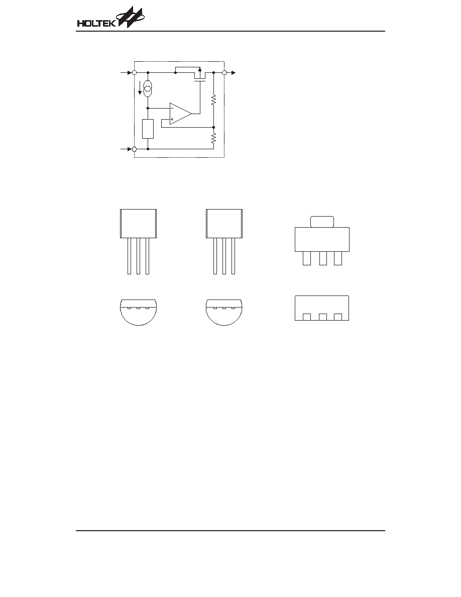
Block Diagram
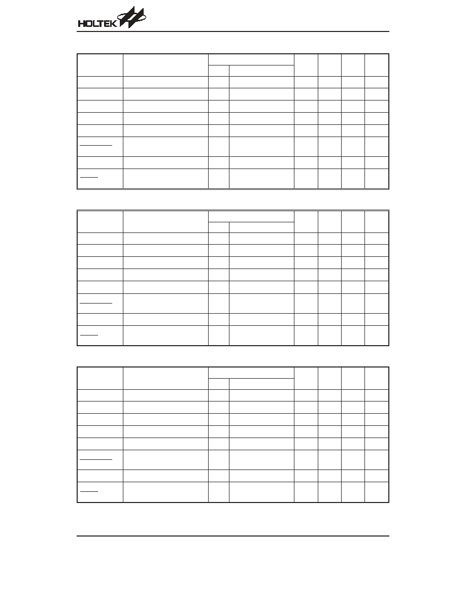
Pin Assignment
Absolute Maximum Ratings
Supply Voltage ...........................V
SS
-0.3V to V
SS
+14V
Storage Temperature ...........................
-50∞C to 125∞C
Power Consumption (*1) .................................. 500mW
Operating Temperature ..........................
-40∞C to 85∞C
Power Consumption (*2) ...................................500mW
Note: These are stress ratings only. Stresses exceeding the range specified under
≤Absolute Maximum Ratings≤ may
cause substantial damage to the device. Functional operation of this device at other conditions beyond those
listed in the specification is not implied and prolonged exposure to extreme conditions may affect device reliabil-
ity.
*1: applied to TO-92
*2: applied to SOT-89
HT73XX
Rev. 1.10
2
July 30, 2004
T O - 9 2 - A
G N D
V I N
V O U T
S O T - 8 9 - A
V O U T
G N D V I N
7 3 X X - A
F r o n t V i e w
B o t t o m V i e w
G N D
V I N
V O U T
7 3 X X - A
T O - 9 2 - B
V O U T
G N D
V I N
7 3 X X - B
F r o n t V i e w
B o t t o m V i e w
V O U T
V I N
G N D
V r e f

Electrical Characteristics
HT7318, +1.8V Output Type
Ta=25
∞C
Symbol
Parameter
Test Conditions
Min.
Typ.
Max.
Unit
V
IN
Conditions
V
OUT
Output Voltage
2.8V
I
OUT
=40mA
1.746
1.8
1.854
V
I
OUT(MAX)
Maximum Output Current
2.8V
V
OUT
≥1.62V
150
æ
æ
mA
DV
OUT
*
Load Regulation
2.8V
1mA
£I
OUT
£60mA
æ
45
90
mV
V
DROP**
Dropout Voltage
æ
I
OUT
=40mA
æ
170
æ
mV
I
SS
Quiescent Current
2.8V
No load
æ
4
8
mA
Line Regulation
æ
I
OUT
=40mA
2.8V
£V
IN
£12V
æ
0.2
0.3
%/V
V
IN
Input Voltage
æ
æ
æ
æ
12
V
Temperature Coefficient
2.8V
I
OUT
=40mA
-40∞C<Ta<85∞C
æ
±0.7
æ
ppm/
∞C
HT7325, +2.5V Output Type
Ta=25
∞C
Symbol
Parameter
Test Conditions
Min.
Typ.
Max.
Unit
V
IN
Conditions
V
OUT
Output Voltage
3.5V
I
OUT
=40mA
2.425
2.5
2.575
V
I
OUT(MAX)
Maximum Output Current
3.5V
V
OUT
≥2.25V
180
æ
æ
mA
DV
OUT
*
Load Regulation
3.5V
1mA
£I
OUT
£60mA
æ
45
90
mV
V
DROP**
Dropout Voltage
æ
I
OUT
=40mA
æ
110
æ
mV
I
SS
Quiescent Current
3.5V
No load
æ
4
8
mA
Line Regulation
æ
I
OUT
=40mA
3.5V
£V
IN
£12V
æ
0.2
0.3
%/V
V
IN
Input Voltage
æ
æ
æ
æ
12
V
Temperature Coefficient
3.5V
I
OUT
=40mA
-40∞C<Ta<85∞C
æ
±0.7
æ
ppm/
∞C
HT7327, +2.7V Output Type
Ta=25
∞C
Symbol
Parameter
Test Conditions
Min.
Typ.
Max.
Unit
V
IN
Conditions
V
OUT
Output Voltage
3.7V
I
OUT
=40mA
2.619
2.7
2.781
V
I
OUT(MAX)
Maximum Output Current
3.7V
V
OUT
≥2.43V
200
æ
æ
mA
DV
OUT
*
Load Regulation
3.7V
1mA
£I
OUT
£80mA
æ
45
90
mV
V
DROP**
Dropout Voltage
æ
I
OUT
=40mA
æ
100
æ
mV
I
SS
Quiescent Current
3.7V
No load
æ
4
8
mA
Line Regulation
æ
I
OUT
=40mA
3.7V
£V
IN
£12V
æ
0.2
0.3
%/V
V
IN
Input Voltage
æ
æ
æ
æ
12
V
Temperature Coefficient
3.7V
I
OUT
=40mA
-40∞C<Ta<85∞C
æ
±0.7
æ
ppm/
∞C
HT73XX
Rev. 1.10
3
July 30, 2004
D V
O U T
D V
I N
¥ V
O U T
D V
O U T
D T
a
D V
O U T
D V
I N
¥ V
O U T
D V
O U T
D T
a
D V
O U T
D T
a
D V
O U T
D V
I N
¥ V
O U T
HT7330, +3.0V Output Type
Ta=25
∞C
Symbol
Parameter
Test Conditions
Min.
Typ.
Max.
Unit
V
IN
Conditions
V
OUT
Output Voltage
4V
I
OUT
=40mA
2.91
3
3.09
V
I
OUT(MAX)
Maximum Output Current
4V
V
OUT
≥2.7V
250
æ
æ
mA
DV
OUT
*
Load Regulation
4V
1mA
£I
OUT
£80mA
æ
45
90
mV
V
DROP
**
Dropout Voltage
æ
I
OUT
=40mA
æ
95
æ
mV
I
SS
Quiescent Current
4V
No load
æ
4
8
mA
Line Regulation
æ
I
OUT
=40mA
4V
£V
IN
£12V
æ
0.2
0.3
%/V
V
IN
Input Voltage
æ
æ
æ
æ
12
V
Temperature Coefficient
4V
I
OUT
=40mA
-40∞C<Ta<85∞C
æ
±0.7
æ
ppm/
∞C
HT7333, +3.3V Output Type
Ta=25
∞C
Symbol
Parameter
Test Conditions
Min.
Typ.
Max.
Unit
V
IN
Conditions
V
OUT
Output Voltage
4.3V
I
OUT
=40mA
3.201
3.3
3.399
V
I
OUT(MAX)
Maximum Output Current
4.3V
V
OUT
≥2.97V
250
æ
æ
mA
DV
OUT
*
Load Regulation
4.3V
1mA
£I
OUT
£80mA
æ
45
90
mV
V
DROP
**
Dropout Voltage
æ
I
OUT
=40mA
æ
90
æ
mV
I
SS
Quiescent Current
4.3V
No load
æ
4
8
mA
Line Regulation
æ
I
OUT
=40mA
4.3V
£V
IN
£12V
æ
0.2
0.3
%/V
V
IN
Input Voltage
æ
æ
æ
æ
12
V
Temperature Coefficient
4.3V
I
OUT
=40mA
-40∞C<Ta<85∞C
æ
±0.7
æ
ppm/
∞C
HT7335, +3.5V Output Type
Ta=25
∞C
Symbol
Parameter
Test Conditions
Min.
Typ.
Max.
Unit
V
IN
Conditions
V
OUT
Output Voltage
4.5V
I
OUT
=40mA
3.395
3.5
3.605
V
I
OUT(MAX)
Maximum Output Current
4.5V
V
OUT
≥3.15V
250
æ
æ
mA
DV
OUT
*
Load Regulation
4.5V
1mA
£I
OUT
£80mA
æ
45
90
mV
V
DROP
**
Dropout Voltage
æ
I
OUT
=40mA
æ
80
æ
mV
I
SS
Quiescent Current
4.5V
No load
æ
4
8
mA
Line Regulation
æ
I
OUT
=40mA
4.5V
£V
IN
£12V
æ
0.2
0.3
%/V
V
IN
Input Voltage
æ
æ
æ
æ
12
V
Temperature Coefficient
4.5V
I
OUT
=80mA
-40∞C<Ta<85∞C
æ
±0.7
æ
ppm/
∞C
HT73XX
Rev. 1.10
4
July 30, 2004
D V
O U T
D V
I N
¥ V
O U T
D V
O U T
D T
a
D V
O U T
D V
I N
¥ V
O U T
D V
O U T
D T
a
D V
O U T
D T
a
D V
O U T
D V
I N
¥ V
O U T
HT7350, +5.0V Output Type
Ta=25
∞C
Symbol
Parameter
Test Conditions
Min.
Typ.
Max.
Unit
V
IN
Conditions
V
OUT
Output Voltage
6V
I
OUT
=40mA
4.85
5
5.15
V
I
OUT(MAX)
Maximum Output Current
6V
V
OUT
≥4.5V
250
æ
æ
mA
DV
OUT
*
Load Regulation
6V
1mA
£I
OUT
£100mA
æ
45
90
mV
V
DROP**
Dropout Voltage
æ
I
OUT
=40mA
æ
60
æ
mV
I
SS
Quiescent Current
6V
No load
æ
4
8
mA
Line Regulation
æ
I
OUT
=40mA
6V
£V
IN
£12V
æ
0.2
0.3
%/V
V
IN
Input Voltage
æ
æ
æ
æ
12
V
Temperature Coefficient
6V
I
OUT
=80mA
-40∞C<Ta<85∞C
æ
±0.7
æ
ppm/
∞C
Note:
≤*≤ Regulation is measured at constant junction temperature, using pulsed ON time.
≤**≤ Dropout is measured at constant junction temperature, using pulsed ON time, and the criterion is V
OUT
in-
side target value
±2%.
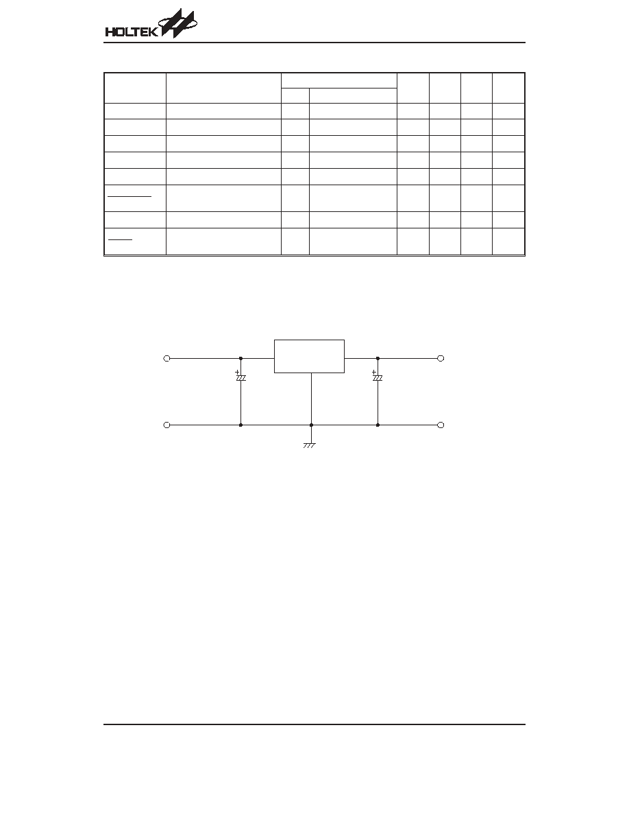
Application Circuits
HT73XX
Rev. 1.10
5
July 30, 2004
C 1
1 0 m F
C o m m o n
C o m m o n
S i n g l e p o i n t G N D
G N D
V
I N
V
I N
V
O U T
V
O U T
C 2
1 0 m F
H T 7 3 X X
S e r i e s
D V
O U T
D V
I N
¥ V
O U T
D V
O U T
D T
a