 | ÐлекÑÑоннÑй компоненÑ: HT7611B | СкаÑаÑÑ:  PDF PDF  ZIP ZIP |
HT761X - General Purpose PIR Controller
HT761X
General Purpose PIR Controller
Selection Table
Part No.
ZC Off/On
for Override
Flash on Mde
Auto-change
Override ON
Duration
Comparator
Window
Effective Trigger
Width
HT7610A
HT7610B
2 times
Flash
8 hrs
1
16
(V
DD
-V
EE
)
>24ms
HT7611A
HT7611B
1 time
No flash
8 hrs
1
16
(V
DD
-V
EE
)
>24ms
Note:
Part numbers suffixed with A are for Relay application while those suffixed with B are for Triac application.
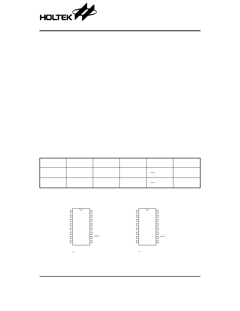
Pin Assignment
Rev. 1.10
1
September 18, 2002
Features
·
Operating voltage: 5V~12V
·
Standby current: 100
mA (Typ.)
·
On-chip regulator
·
Adjustable output duration
·
CDS input
·
40 second warm-up
·
ON/AUTO/OFF selectable by MODE pin
·
Override function
·
Auto-reset if the ZC signal disappears over 3
seconds
·
16-pin DIP package
General Description
The HT761X is a CMOS LSI chip designed for use in au-
tomatic PIR lamp control. It can operate with a 2-wire
configuration for triac applications or with a 3-wire con-
figuration for relay applications. The chip is equipped
with operational amplifiers, a comparator, timer, a zero
crossing detector, control circuit, a voltage regulator, a
system oscillator, and an output timing oscillator.
Its PIR sensor detects infrared power variations induced
by the motion of a human body and transforms it to a
voltage variation. If the PIR output voltage variation con-
forms to the criteria (refer to the functional description),
the lamp is turned on with an adjustable duration.
The HT761X offers three operating modes (ON, AUTO,
OFF) which can be set through the MODE pin. While the
chip is working in the AUTO mode the user can override
it and switch to the TEST mode, or manual ON mode, or
return to the AUTO mode by switching the power switch.
Applications
·
PIR light controllers
·
Motion detectors
·
Alarm systems
·
Auto door bells
H T 7 6 1 X A
1 6 D I P - B
R E L A Y V E R S I O N
H T 7 6 1 X B
1 6 D I P - A
T R I A C V E R S I O N
V S S
R E L A Y
O S C D
O S C S
Z C
C D S
M O D E
V D D
O P 2 O
O P 2 N
O P 2 P
O P 1 O
O P 1 N
O P 1 P
V E E
V S S
T R I A C
O S C D
O S C S
Z C
C D S
M O D E
V D D
O P 2 O
O P 2 N
O P 2 P
O P 1 O
O P 1 N
O P 1 P
R S T
V E E
1
2
3
4
5
6
7
8
1 6
1 5
1 4
1 3
1 2
1 1
1 0
9
1
2
3
4
5
6
7
8
1 6
1 5
1 4
1 3
1 2
1 1
1 0
9
R S T
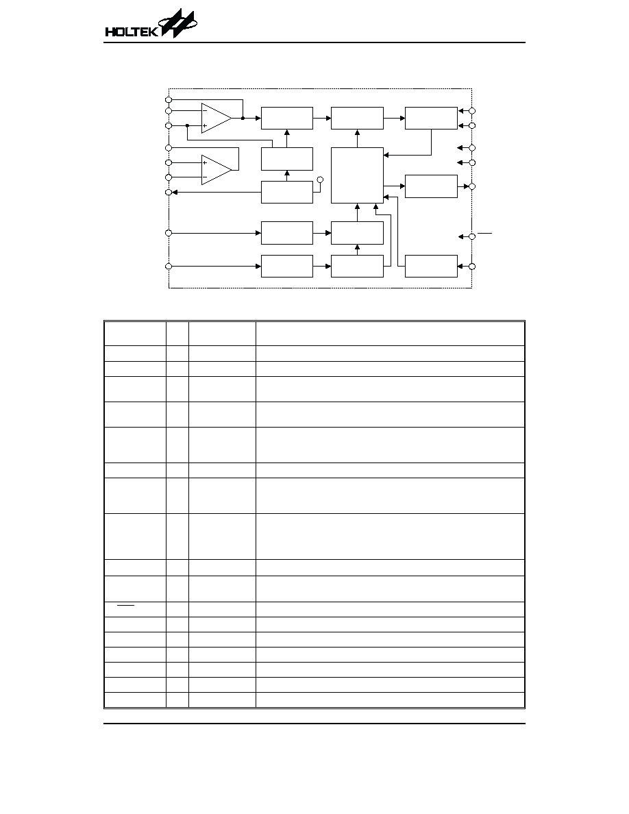
Block Diagram
Pin Description
Pin Name
I/O
Internal
Connection
Description
VSS
¾
¾
Negative power supply, ground
RELAY
O
CMOS
RELAY drive output through an external NPN transistor, active high.
TRIAC
O
CMOS
TRIAC drive output
The output is a pulse output when active.
OSCD
I/O
PMOS IN
NMOS OUT
Output timing oscillator I/O
It is connected to an external RC to adjust output duration.
OSCS
I/O
PMOS IN
NMOS OUT
System oscillator I/O
OSCS is connected to an external RC to set the system frequency. The
system frequency is at 16kHz for normal application.
ZC
I
CMOS
Input for AC zero crossing detection
CDS
I
CMOS
CDS is connected to a CDS voltage divider for daytime/night
auto-detection. Low input to this pin can disable the PIR input. CDS a
Schmitt Trigger input with 5-second input debounce time.
MODE
I
CMOS
Operating mode selection input:
VDD: Output is always ON
VSS: Output is always OFF
Open: Auto detection
VDD
¾
¾
Positive power supply
VEE
O
NMOS
Regulated voltage output
The output voltage is
-4V with respect to VDD.
RST
I
Pull-High
Chip reset input, active low
OP1P
I
PMOS
Noninverting input of OP1
OP1N
I
PMOS
Inverting input of OP1
OP1O
O
NMOS
Output of OP1
OP2P
I
PMOS
Noninverting input of OP2
OP2N
I
PMOS
Inverting input of OP2
OP2O
O
NMOS
Output of OP2
HT761X
Rev. 1.10
2
September 18, 2002
V o l t a g e
D i v i d e r
C o m p a r a t o r
O P 2 N
O P 2 P
O P 2 O
O P 1 P
O P 1 N
V E E
O P 1 O
L a t c h C i r c u i t
M o d e & C D S
C i r c u i t
R e g u l a t o r
C o n t r o l
C i r c u i t
O u t p u t C i r c u i t
R E L A Y
( T R I A C )
D e l a y C i r c u i t
C o u n t e r
C i r c u i t
Z e r o C r o s s
D e b o u n c e
D e l a y
O s c i l l a t o r
S y s t e m
O s c i l l a t o r
O S C D
O S C S
R S T
M O D E
C D S
V D D
V S S
Z C
V
D D
Absolute Maximum Ratings
Supply Voltage .........................................
-0.3V to 13V
Storage Temperature ...........................
-50°C to 125°C
Input Voltage .............................V
SS
-0
.
3V to V
DD
+0.3V
Operating Temperature ..........................
-25°C to 70°C
Zero Crossing Current ................................Max. 300
mA
Note: These are stress ratings only. Stresses exceeding the range specified under
²Absolute Maximum Ratings² may
cause substantial damage to the device. Functional operation of this device at other conditions beyond those
listed in the specification is not implied and prolonged exposure to extreme conditions may affect device reliabil-
ity.
Electrical Characteristics
Symbol
Parameter
Test Condition
Min.
Typ.
Max.
Unit
V
DD
Condition
V
DD
Operating Voltage
¾
¾
5
9
12
V
V
EE
Regulator Output Voltage
12V
V
DD
-V
EE
3.5
4
4.5
V
I
DD
Operating Current
12V
No load, OSC on
¾
100
350
mA
I
OH1
OUTPUT Source Current
(RELAY, TRIAC)
12V
V
OH
=10.8V
-6
12
¾
mA
I
OL1
OUTPUT Sink Current
(RELAY, TRIAC)
12V
V
OL
=1.2V
40
80
¾
mA
I
OL2
VEE Sink Current
12V
V
DD
-VEE
=4V
¾
¾
¾
mA
V
IH
²H² Input Voltage
¾
¾
0.8V
DD
¾
¾
V
V
IL
²L² Input Voltage
¾
¾
¾
¾
0.2V
DD
V
V
TH1
CDS
²H² Transfer Voltage
12V
¾
6.4
8
9.6
V
V
TL1
CDS
²L² Transfer Voltage
12V
¾
3.7
4.7
5.6
V
V
TH2
ZC
²H² Transfer Voltage
12V
¾
4.7
6.7
8.7
V
V
TL2
ZC
²L² Transfer Voltage
12V
¾
1.3
1.8
2.3
V
V
OS
OP Amp Input Offset Voltage
12V
No load
¾
10
35
mV
f
SYS
System Oscillator Frequency
12V
R
OSCS
=560k
W
C
OSCS
=100pF
12.8
16
19.2
KHz
f
d
Delay Oscillator Frequency
12V
R
OSCD
=560k
W
C
OSCD
=100pF
12.8
16
19.2
KHz
A
VO
OP Amp Open Loop Gain
12V
No load
60
80
¾
dB
HT761X
Rev. 1.10
3
September 18, 2002
Functional Description
VEE
VEE supplies power to the analog front end cir-
cuit with a normally stabilized voltage of
-4V
with respect to VDD.
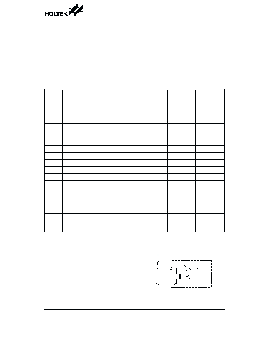
OSCS
OSCS is a system oscillator input pin. When it is
connected to an external RC, a system fre-
quency of 16kHz can be generated.
O S C S
V
D D
C
S
1 0 0 p .
R
S
5 6 0 k W
System oscillator
HT761X
Rev. 1.10
4
September 18, 2002
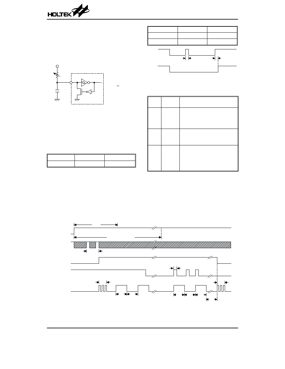
OSCD
OSCD is an output timing oscillator input pin. It is con-
nected to an external RC to obtain the desired output
turn-on duration. Variable output turn-on durations can
be achieved by selecting various values of RC or using a
variable resistor.
RELAY (TRIAC)
RELAY is an output pin set as a RELAY driving (active
high) output for the HT761XA, or as a TRIAC driving (ac-
tive low) output for the HT761XB.
The output active duration is controlled by the OSCD os-
cillating period.
HT761XA
HT761XB
OUTPUT
RELAY
TRIAC
CDS
CDS is a CMOS Schmitt Trigger input structure. It is
used to distinguish between day time and night time.
When the input voltage of CDS is high the PIR input is
enabled. On the other hand, when CDS is low the PIR
input is disabled. The input disable to enable debounce
time is 5 seconds. Connect this pin to VDD when this
function is not used. The CDS input is ignored when the
output is active.
CDS
Status
PIR
LOW
Day Time
Disabled
HIGH
Night
Enabled
MODE
MODE is a tristate input pin used to select the operating
mode.
MODE
Status
Operating
Mode
Description
VDD
ON
Output is always ON:
RELAY outputs high for relay driving.
TRIAC pulse train output is syn-
chronized by ZC for triac driving.
VSS
OFF
Output is always OFF:
RELAY outputs low for relay driving.
TRIAC outputs high for triac driving.
Open
AUTO
Outputs remain in the off state until
activated by a valid PIR input trigger
signal. When working in the AUTO
mode, the chip allows override con-
trol by switching the ZC signal.
R
D
C
D
O S C D
V
D D
Output timing oscillator
T
D
=
1
f
´ 21504
< 5 s e c
d i s a b l e
C D S
P I R
e n a b l e
5 s e c
e n a b l e
R S T B
Z C
T e s t
e n a b l e
C o m p a r a t o r
o u t p u t
R E L A Y
( T R I A C )
1 0 s
4 0 s w a r m - u p t i m e
< 3 s
O . . / O N o n e o r t w o t i m e s b y m a s k o p t i o n
> 0 . 3 4 s
O N
f l a s h o r n o t b y m a s k o p t i o n
O N
O N
O N
> 3 2 s
*
f l a s h 3 t i m e s i n 1 H z
O . .
#
2 s
2 s
2 s
* : f l a s h 3 t i m e s a t a 1 H z r a t e
f l a s h o r n o t b y m a s k o p t i o n
# : f l a s h 3 t i m e s a t a 2 H z r a t e
f l a s h o r n o t b y m a s k o p t i o n
2 s
2 s
HT761X
Rev. 1.10
5
September 18, 2002
ZC
ZC is a CMOS input structure. It receives AC line fre-
quency and generates zero crossing pulses to synchro-
nize the triac driver. By effective ZC signal switching
(switch OFF/ON 1 or 2 times within 3 seconds by mask
option), the chip provides the following additional func-
tions:
·
Test mode control
Within 10 seconds after power-on, effective ZC
switching will force the chip to enter the test mode.
During the test mode, the outputs will be active for a
duration of 2 seconds each time a valid PIR trigger
signal is received. If a time interval exceeds 32 sec-
onds without a valid trigger input, the chip will auto-
matically enter the AUTO mode.
·
Override control
When the chip is working in an AUTO mode
(MODE=open), the output is activated by a valid PIR
trigger signal and the output active duration is con-
trolled by an OSCD oscillating period. The lamp can
be switched always to
²ON² from the AUTO mode by
either switching the MODE pin to VDD or switching
the ZC signal by an OFF/ON operation of the power
switch (OFF/ON once or twice within 3 seconds by
mask option). The term
²override² refers to the
change of operating mode by switching the power
switch. The chip can be toggled from ON to AUTO by
an override operation. If the chip is overridden to ON
and there is no further override operation, it will auto-
matically return to AUTO after an internal preset ON
time duration has elapsed. This override ON time du-
ration can be set to 4 or 6 or 8 hours by mask option.
The default is 8 hours.
The chip provides a mask option to determine the out-
put flash times (3 times) when changing the operating
mode. It will flash 3 times at a 1Hz rate each time the
chip changes from an AUTO mode to another mode or
flash 3 times at a 2Hz rate when returning to the
AUTO mode. But if the AUTO mode is changed by
switching the MODE switch it will not flash.
RST
RST is used to reset the chip. It is internal pull-high and
active low.
The use of C
RST
can extend the power-on initial time. If
the RST pin is an open circuit (without C
RST
), the initial
time is the default (40 secs).
Power on initial
The PIR signal amplifier requires a warm up period after
power-on. The input should be disabled during this pe-
riod.
In the AUTO mode within the first 10 seconds of
power-on initialization, the chip allows override control
to enter the test mode. After 40 seconds of the initial
time the chip allows override control between ON and
AUTO. It will remain in the warm up period if the total ini-
tial time has not elapsed after returning to AUTO.
In case that the ZC signal disappears for more than 3
seconds, the chip will restart the initialization operation.
However, the restart initial time is always 40 seconds
and cannot be extended by adding C
RST
to the RST pin
as shown in the Fig.1.
Mask options
The HT761X offers mask options to select the output
flash (3 times) when changing the operating mode. The
chip will flash 3 times at a 1Hz rate each time it changes
from AUTO to another mode and flash 3 times at a 2Hz
rate when it returns to the AUTO mode. However the
chip will not flash if the mode is changed by switching
the MODE switch.
·
4, 6, or 8 hour options to return to AUTO from override
ON. The default is 8 hours.
·
Options for effective override: Once or twice OFF/ON
operation of power switch within 3 seconds. The de-
fault is OFF/ON twice.
·
Options for output flash to indicate effective override
operation. The default is to flash.
·
Options for effective PIR trigger pulse width: >24mS,
>32mS or >48mS. The default is 24ms.
Z C
A U T O
O N
A U T O
A U T O
O p e r a t i n g
M o d e
4 , 6 o r 8 h r b y m a s k o p t i o n
O N
f l a s h
f l a s h
f l a s h
f l a s h
ZC override timing
R E S T
R S T
1 0 0 m .
C
R S T
V C C
V E E
V
D D
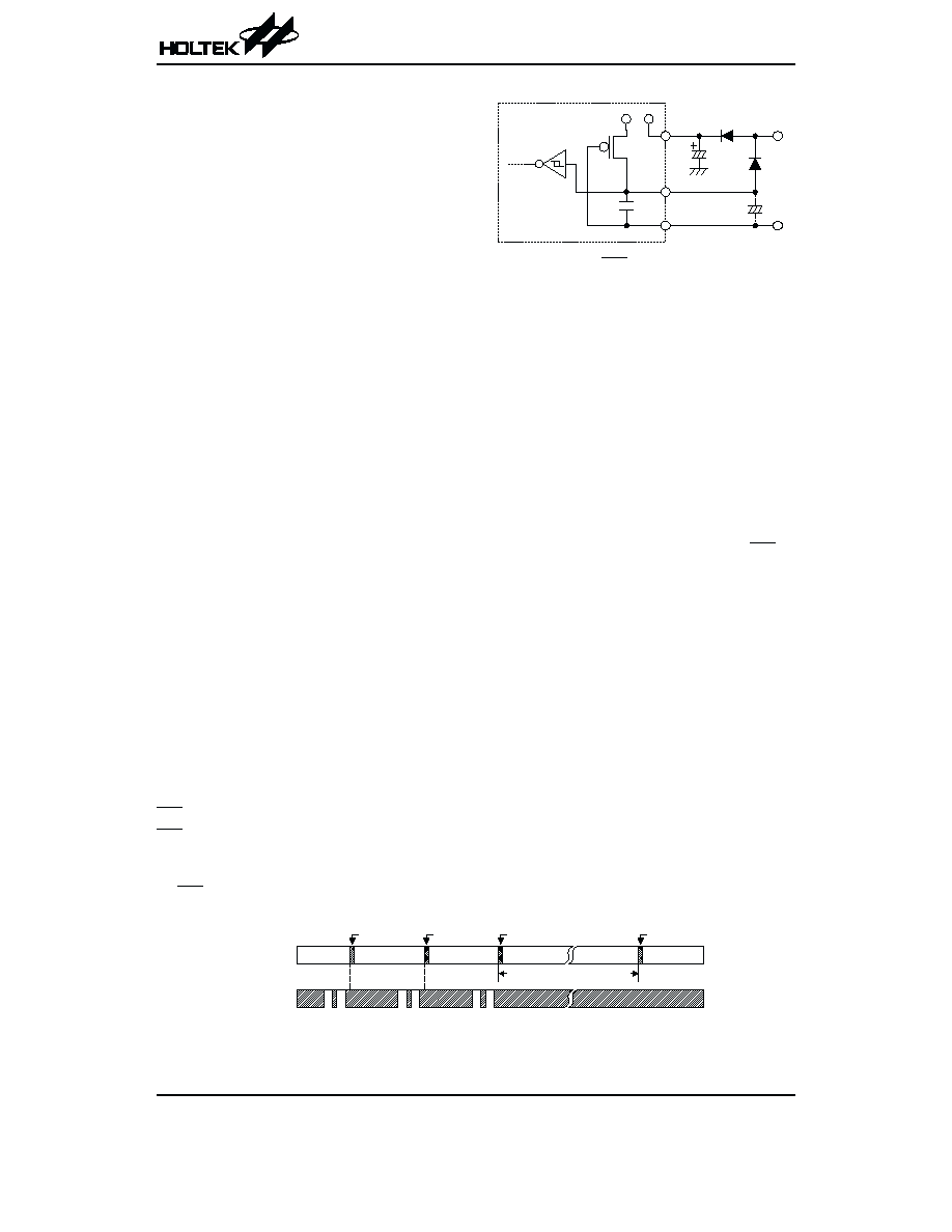
Fig.1 RST application example
Document Outline
- þÿ
- þÿ
- þÿ
- þÿ
- þÿ
- þÿ
- þÿ
- þÿ
- þÿ
- þÿ
- þÿ
- þÿ
- þÿ