HT82V14
14-Bit CCD/CIS Analog Signal Processor
Block Diagram
1
July 12, 2000
Features
∑
Low power CMOS : 350 mW
∑
9 ADC clock latency for digital data output
∑
14-bit 6 MSPS A/D converter
∑
3-channel correlated double sampler
∑
1~6 programmable gain
∑
Input clamp circuitry for CDS-mode
∑
Internal/external circuitfor CIS
∑
Internal/external voltage reference
∑
Internal MUX for channel operation
∑
1 or 3-channel operation
∑
Pixel-rate or line-rate switch operation
∑
Programmable 3-wire serial interface
∑
+5V digital I/O compatibility
∑
28-pin SOP/SOJ package
C L P
C L P
C L P
C D S
C D S
C D S
3
¥
2 b i t s
C o a r s e
G a i n
3
¥
8 b i t s
D A C
O f f s e t
V G A
+
+
+
V G A
V G A
M U X
1 4 - b i t
A D C
P G A
3
¥
5 b i t s
F i n e
G a i n
C o n f i g
R e g i s t e r
C o n t r o l
P o r t
D 1 3 ~ D 0
S C L K
C S
S D A T A
P i x e l R a t e
G u a r a n t e e
O E
V o l t a g e R e f e r e n c e
O F F S E T R E F T C M L R E F
C D S C L K 1
C D S C L K 2
A D C C L K
R I N
G I N
B I N
General Description
The HT82V14 is a complete analog signal pro-
cessor for CCD imaging applications. It fea-
tures a 3-channel architecture designed to
sample and condition the outputs of the
trilinear color CCD arrays. Each channel con-
sists of an input clamp, Correlated Double
Sampler (CDS), offset DAC and Programmable
Gain Amplifier (PGA), multiplexed to a high
performance 14-bit A/D converter.
The CDS amplifiers may be disabled for use
with sensors such as Contact Image Sensors
(CIS) and CMOS active pixel sensors, which do
not require CDS.
The 14-bit digital output is multiplexed into an
8-bit output word that is accessed using two
read cycles. The internal registers are pro-
grammed through a 3-wire serial interface,
which provides gain, offset, and operating mode
adjustments.

Pin Assignment
Pin Description
Pin No.
Pin Name
I/O
Description
1
CDSCLK1
DI
CDS reset clock pulse input
2
CDSCLK2
DI
CDS data clock pulse input
3
ADCCLK
DI
A/D sample clock input for 3-channels mode
4
OE
DI
Output enable
5
DRVDD
æ
Digital driver power
6
DRVSS
æ
Digital driver ground
14~7
D0~D13
DO
Digital data output
15
SDATA
DIO
Serial data input/output
16
SCLK
DI
Clock input for serial interface
17
CS
DI
Chip select
18, 27
AVSS
æ
Analog ground
19, 28
AVDD
æ
+5V analog supply
20
REF
AO
Reference decoupling
21
REFT
AO
Reference decoupling
22
BIN
AI
Analog Input, blue
23
CML
AO
Internal reference output
24
GIN
AI
Analog Input, green
25
OFFSET
AO
CIS reference decoupling
26
RIN
AI
Analog input, red
HT82V14
2
July 12, 2000
2 8
2 7
2 6
2 5
2 4
2 3
2 2
2 1
2 0
1 9
1 8
1 7
1 6
1 5
1
2
3
4
5
6
7
8
9
1 0
1 1
1 2
1 3
1 4
A V D D
A V S S
R I N
O F F S E T
G I N
C M L
B I N
R E F T
R E F
A V S S
A V D D
S L O A D
S C L K
S D A T A
C D S C L K 1
C D S C L K 2
A D C C L K
O E
D R V D D
D R V S S
D 1 3 / D 5
D 1 2 / D 4
D 1 1 / D 3
D 1 0 / D 2
D 9 / D 1
D 8 / D 0
D 7
D 6
H T 8 2 V 1 4
2 8 S O P / S O J

Absolute Maximum Ratings
Supply Voltage .............................-0.3V to 5.5V
Storage Temperature ......................0∞C to 70∞C
Input Voltage ................V
SS
-0.3V to V
DD
+0.3V
Operating Temperature ...............25∞C to 50∞C
Note: These are stress ratings only. Stresses exceeding the range specified under ≤Absolute Maxi-
mum Ratings≤ may cause substantial damage to the device. Functional operation of this device
at other conditions beyond those listed in the specification is not implied and prolonged expo-
sure to extreme conditions may affect device reliability.
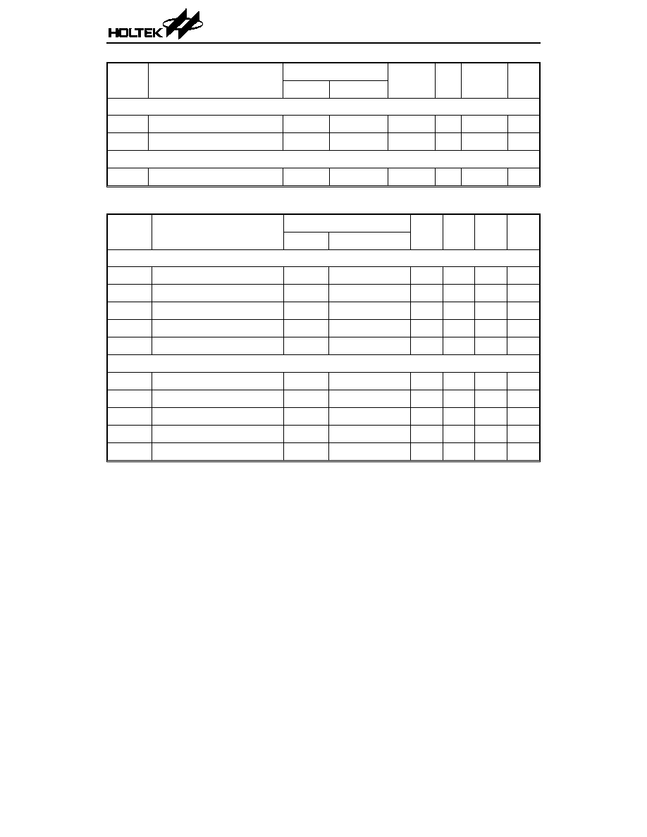
Electrical Characteristics
Symbol
Parameter
Test Conditions
Min.
Typ.
Max.
Unit
V
DD
Conditions
Conversion Rate
3-channel Mode with CDS
5V±10%
æ
æ
æ
6
MSPS
1-channel Mode with CDS
5V±10%
æ
æ
æ
5
MSPS
A/D Converter
Resolution
5V±10%
æ
æ
14
æ
BIT
Integral Nonlinearity
(INL)
5V±10%
æ
æ
±4.5
æ
LSB
Differential Nonlinearity
(DNL)
5V±10%
æ
-0.5
æ
1.2
LSB
Analog Inputs
Full-scale Input Range
5V±10%
æ
æ
4
æ
Vp-p
Input Limits
5V±10%
æ
AV
DD
-0.3 æ AV
DD
+0.3
V
Input Capacitance
5V±10%
æ
æ
TBD
æ
pF
Input Current
5V±10%
æ
æ
TBD
æ
mA
Amplifiers
Coarse Gain Range
5V±10%
æ
1
æ
3
V/V
Coarse Gain Resolution
5V±10%
æ
æ
2
æ
Bits
PGA Gain Range
5V±10%
æ
1
æ
2
V/V
PGA Gain Resolution
5V±10%
æ
æ
5
æ
Bits
Offset Range
5V±10%
æ
-200
æ
200
mV
Offset Resolution
5V±10%
æ
æ
8
æ
Bits
HT82V14
3
July 12, 2000

Timing Diagrams
Timing Mode Sensor Mode
Channel Mode
A
CDS
3-channel internally-defined and pixel-rate mux (00)
B
CDS
1-channel internally-defined mux (01)
C
CIS/SHA
3-channel internally-defined and pixel-rate mux (00)
D
CIS/SHA
1-channel internally-defined mux (01)
Mode A
Note: DATA timing from pixel to pixel is decided by the first rising edge of ADCCLK when
CDSCLK2 is from high to low.
Mode B
HT82V14
5
July 12, 2000
R ( n - 4 )
D 1 3 ~ D 6
R ( n - 4 )
D 5 ~ D 0
G ( n - 4 )
D 1 3 ~ D 6
G ( n - 4 )
D 5 ~ D 0
B ( n - 4 )
D 1 3 ~ D 6
B ( n - 4 )
D 5 ~ D 0
R ( n - 3 )
D 1 3 ~ D 6
R ( n - 3 )
D 5 ~ D 0
G ( n - 3 )
D 1 3 ~ D 6
G ( n - 3 )
D 5 ~ D 0
B ( n - 3 )
D 1 3 ~ D 6
B ( n - 3 )
D 5 ~ D 0
R ( n - 2 )
D 1 3 ~ D 6
R ( n - 2 )
D 5 ~ D 0
R
G
B
R
G
B
R
G
B
C D S C L K 1
C D S C L K 2
A D C C L K
D 1 3 ~ D 0
A n a l o g I n p u t
t
C P
t
N V P
t
S T L 1
t
N V P
t
C 2 A
P i x e l n
P i x e l n + 1
t
A D
t
A D
t
C 1 A
t
C 1 C 2 A
t
C 2 C 1 A
t
C R A
C D S C L K 1
D 1 3 ~ D 0
A n a l o g I n p u t
P i x e l n
P i x e l n + 1
t
A D
P i x e l n + 2
C D S C L K 2
D ( n - 1 0 )
D 1 3 ~ D 6
D ( n - 1 0 )
D 5 ~ D 0
D ( n - 8 )
D 1 3 ~ D 6
D ( n - 9 )
D 5 ~ D 0
t
C 1 B
t
C 2 C 1 B
t
C 2 B
t
C 1 C 2 B
t
A D
t
C R B
D ( n - 9 )
D 1 3 ~ D 6